ZHCSL66 April   2020 TPS7B81

PRODUCTION DATA.  

  1. 特性
  2. 应用
  3. 说明
    1.     Device Images
      1.      T48 路多路复用 LC6948
      2.      静态电流与环境温度间的关系 (VOUT = 3.3V)
  4. 修订历史记录
  5. Pin Configuration and Functions
    1.     Pin Functions
  6. Specifications
    1. 6.1 Absolute Maximum Ratings
    2. 6.2 ESD Ratings
    3. 6.3 Recommended Operating Conditions
    4. 6.4 Thermal Information
    5. 6.5 Electrical Characteristics
    6. 6.6 Typical Characteristics
  7. Detailed Description
    1. 7.1 Overview
    2. 7.2 Functional Block Diagram
    3. 7.3 Feature Description
      1. 7.3.1 Device Enable (EN)
      2. 7.3.2 Undervoltage Shutdown
      3. 7.3.3 Current Limit
      4. 7.3.4 Thermal Shutdown
    4. 7.4 Device Functional Modes
      1. 7.4.1 Operation With VIN Lower Than 3 V
      2. 7.4.2 Operation With VIN Larger Than 3 V
  8. Application and Implementation
    1. 8.1 Application Information
      1. 8.1.1 Power Dissipation
        1. 8.1.1.1 Estimating Junction Temperature
    2. 8.2 Typical Application
      1. 8.2.1 Design Requirements
      2. 8.2.2 Detailed Design Procedure
        1. 8.2.2.1 Input Capacitor
        2. 8.2.2.2 Output Capacitor
      3. 8.2.3 Application Curve
  9. Power Supply Recommendations
  10. 10Layout
    1. 10.1 Layout Guidelines
    2. 10.2 Layout Example
  11. 11器件和文档支持
    1. 11.1 接收文档更新通知
    2. 11.2 支持资源
    3. 11.3 商标
    4. 11.4 静电放电警告
    5. 11.5 Glossary
  12. 12机械、封装和可订购信息

封装选项

机械数据 (封装 | 引脚)
散热焊盘机械数据 (封装 | 引脚)
订购信息

Typical Characteristics

at TJ = –40°C to +150°C, VIN = 14 V, and VEN ≥ 2 V (unless otherwise noted)
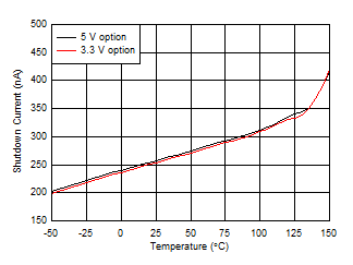
TPS7B81 shutdown_current_vs_temp.gif
VEN = 0 V
Figure 1. Shutdown Current vs Ambient Temperature
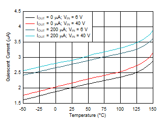
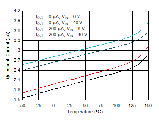
TPS7B81 iq_vs_temp_3v3.gif
VOUT = 3.3 V
Figure 3. Quiescent Current vs Ambient Temperature
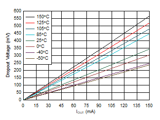
TPS7B81 dropout_vs_iout_3v3.gif
VOUT = 3.3 V, DRV package
Figure 5. Dropout Voltage vs Output Current
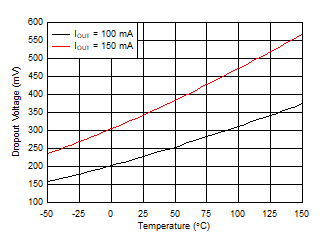
TPS7B81 dropout_vs_temp_3v3.gif
VOUT = 3.3 V
Figure 7. Dropout Voltage vs Ambient Temperature
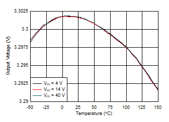
TPS7B81 accuracy_vs_temp_3v3.gif
VOUT = 3.3 V, IOUT = 1 mA
Figure 9. Output Voltage vs Ambient Temperature
TPS7B81 25_to_150_acc_hist_v2.gif
3.3-V and 5-V options, IOUT = 1 mA
Figure 11. Temperature Drift Histogram (25ºC to 150ºC)
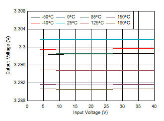
TPS7B81 accuracy_vs_vin_3v3.gif
VOUT = 3.3 V, IOUT = 1 mA
Figure 13. Output Voltage vs Input Voltage
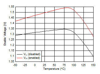
TPS7B81 enable_voltage_vs_temp.gif
Figure 15. Enable Voltage vs Ambient Temperature
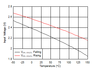
TPS7B81 uvlo_vs_temp.gif
Figure 17. UVLO vs Ambient Temperature
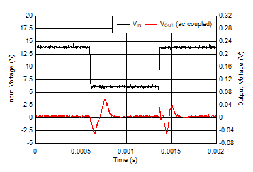
TPS7B81 D004_line_transient.gif
VOUT = 3.3 V, CIN = 0 µF, COUT = 1 µF,
IOUT = 100 mA, slew rate = 1 V/µs
Figure 19. Line Transient
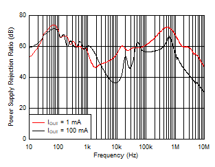
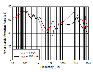
TPS7B81 psrr_5v.gif
VOUT = 5 V, CIN = 0 µF, COUT = 10 µF
Figure 21. PSRR vs Frequency
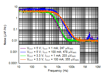
TPS7B81 noise.gif
CIN = 0.1 µF, COUT = 10 µF
Figure 23. Noise vs Frequency
TPS7B81 iq_vs_temp_5v.gif
VOUT = 5 V
Figure 2. Quiescent Current vs Ambient Temperature
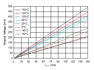
TPS7B81 dropout_vs_iout_5v.gif
VOUT = 5 V, DRV package
Figure 4. Dropout Voltage vs Output Current
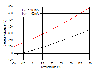
TPS7B81 dropout_vs_temp_5v.gif
VOUT = 5 V
Figure 6. Dropout Voltage vs Ambient Temperature
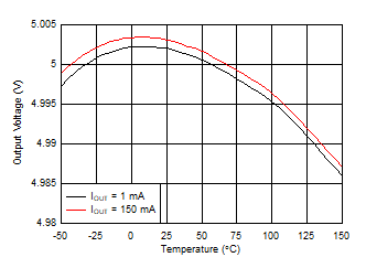
TPS7B81 accuracy_vs_temp_5v.gif
VOUT = 5 V
Figure 8. Output Voltage vs Ambient Temperature
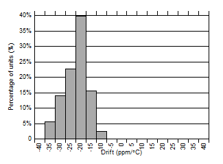
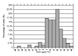
TPS7B81 neg40_to_25_acc_hist_v2.gif
3.3-V and 5-V options, IOUT = 1 mA
Figure 10. Temperature Drift Histogram (–40°C to +25°C)
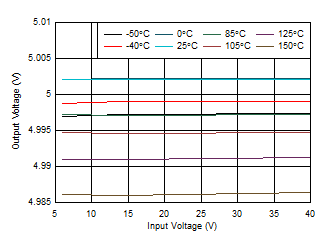
TPS7B81 accuracy_vs_vin_5v.gif
VOUT = 5 V, IOUT = 1 mA
Figure 12. Output Voltage vs Input Voltage
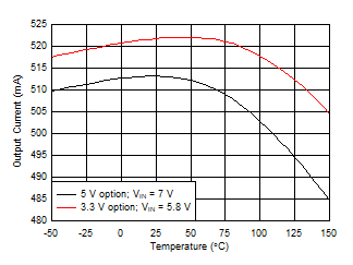
TPS7B81 current_limit_vs_temp.gif
VOUT is shorted to 90% × VOUT(NOM)
Figure 14. Output Current Limit vs Ambient Temperature
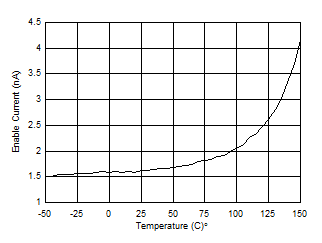
TPS7B81 enable_current_vs_temp.gif
Figure 16. Enable Current vs Ambient Temperature
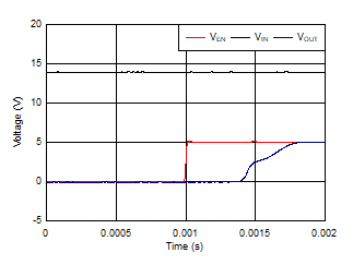
TPS7B81 D005_startup.gif
VOUT = 5 V, CIN = 1 µF, COUT = 1 µF
Figure 18. Startup With Enable
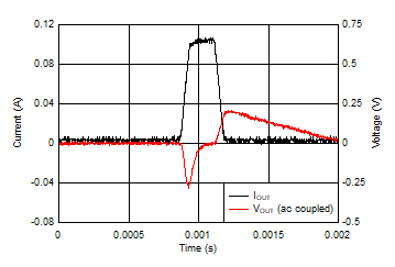
TPS7B81 D006_load_transient.gif
VOUT = 5 V, CIN = 1 µF, COUT = 1 µF,
IOUT = 1 mA → 100 mA → 1 mA, slew rate = 1 mA/µs
Figure 20. Load Transient
TPS7B81 psrr_3v3.gif
VOUT = 3.3 V, CIN = 0 µF, COUT = 10 µF
Figure 22. PSRR vs Frequency
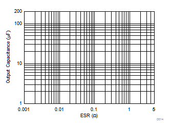
TPS7B81 D014_SLVSDQ0.gif
Figure 24. Output Capacitance vs ESR Stability