ZHCSLG3C June   2020  – August 2022 TPS7B86-Q1

PRODUCTION DATA  

  1. 特性
  2. 应用
  3. 说明
  4. Revision History
  5. Pin Configuration and Functions
  6. Specifications
    1. 6.1 Absolute Maximum Ratings
    2. 6.2 ESD Ratings
    3. 6.3 Recommended Operating Conditions
    4. 6.4 Thermal Information
    5. 6.5 Electrical Characteristics
    6. 6.6 Switching Characteristics
    7. 6.7 Typical Characteristics
  7. Detailed Description
    1. 7.1 Overview
    2. 7.2 Functional Block Diagrams
    3. 7.3 Feature Description
      1. 7.3.1 Enable (EN)
      2. 7.3.2 Power-Good (PG)
      3. 7.3.3 Adjustable Power-Good Delay Timer (DELAY)
      4. 7.3.4 Undervoltage Lockout
      5. 7.3.5 Thermal Shutdown
      6. 7.3.6 Current Limit
    4. 7.4 Device Functional Modes
      1. 7.4.1 Device Functional Mode Comparison
      2. 7.4.2 Normal Operation
      3. 7.4.3 Dropout Operation
      4. 7.4.4 Disabled
  8. Application and Implementation
    1. 8.1 Application Information
      1. 8.1.1 Input and Output Capacitor Selection
      2. 8.1.2 Adjustable Device Feedback Resistor Selection
      3. 8.1.3 Feed-Forward Capacitor
      4. 8.1.4 Dropout Voltage
      5. 8.1.5 Reverse Current
      6. 8.1.6 Power Dissipation (PD)
        1. 8.1.6.1 Thermal Performance Versus Copper Area
        2. 8.1.6.2 Power Dissipation Versus Ambient Temperature
      7. 8.1.7 Estimating Junction Temperature
      8. 8.1.8 Power-Good
        1. 8.1.8.1 Setting the Adjustable Power-Good Delay
    2. 8.2 Typical Application
      1. 8.2.1 Design Requirements
      2. 8.2.2 Detailed Design Procedure
        1. 8.2.2.1 Input Capacitor
        2. 8.2.2.2 Output Capacitor
      3. 8.2.3 Application Curves
    3. 8.3 Power Supply Recommendations
    4. 8.4 Layout
      1. 8.4.1 Layout Guidelines
        1. 8.4.1.1 Package Mounting
        2. 8.4.1.2 Board Layout Recommendations to Improve PSRR and Noise Performance
      2. 8.4.2 Layout Examples
  9. Device and Documentation Support
    1. 9.1 Device Support
      1. 9.1.1 Device Nomenclature
    2. 9.2 接收文档更新通知
    3. 9.3 支持资源
    4. 9.4 Trademarks
    5. 9.5 Electrostatic Discharge Caution
    6. 9.6 术语表
  10. 10Mechanical, Packaging, and Orderable Information

封装选项

机械数据 (封装 | 引脚)
散热焊盘机械数据 (封装 | 引脚)
订购信息

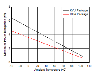
Power Dissipation Versus Ambient Temperature

Figure 8-6 is based off of a JESD51-7 4-layer, high-K board. The allowable power dissipation was estimated using the following equation. As discussed in the An empirical analysis of the impact of board layout on LDO thermal performance application note, thermal dissipation can be improved in the JEDEC high-K layout by adding top layer copper and increasing the number of thermal vias. If a good thermal layout is used, the allowable thermal dissipation can be improved by up to 50%.

Equation 8. GUID-20201021-CA0I-QC5G-DT5Q-9CXMF9K2QPZJ-low.gif
GUID-20201124-CA0I-KKSD-9VBP-NG63HFP0SKLD-low.gif Figure 8-6 TPS7B86-Q1 Allowable Power Dissipation