ZHCSMK8A December   2020  – April 2021 TPS7B87-Q1

PRODUCTION DATA  

  1. 特性
  2. 应用
  3. 说明
  4. Revision History
  5. Pin Configuration and Functions
  6. Specifications
    1. 6.1 Absolute Maximum Ratings
    2. 6.2 ESD Ratings
    3. 6.3 Recommended Operating Conditions
    4. 6.4 Thermal Information
    5. 6.5 Electrical Characteristics
    6. 6.6 Switching Characteristics
    7. 6.7 Typical Characteristics
  7. Detailed Description
    1. 7.1 Overview
    2. 7.2 Functional Block Diagram
    3. 7.3 Feature Description
      1. 7.3.1 Power-Good (PG)
      2. 7.3.2 Adjustable Power-Good Delay Timer (DELAY)
      3. 7.3.3 Undervoltage Lockout
      4. 7.3.4 Thermal Shutdown
      5. 7.3.5 Current Limit
    4. 7.4 Device Functional Modes
      1. 7.4.1 Device Functional Mode Comparison
      2. 7.4.2 Normal Operation
      3. 7.4.3 Dropout Operation
      4. 7.4.4 Disabled
  8. Application and Implementation
    1. 8.1 Application Information
      1. 8.1.1 Input and Output Capacitor Selection
      2. 8.1.2 Dropout Voltage
      3. 8.1.3 Reverse Current
      4. 8.1.4 Power Dissipation (PD)
        1. 8.1.4.1 Thermal Performance Versus Copper Area
        2. 8.1.4.2 Power Dissipation Versus Ambient Temperature
      5. 8.1.5 Estimating Junction Temperature
      6. 8.1.6 Pulling Up the PG Pin to a Different Voltage
      7. 8.1.7 Power-Good
        1. 8.1.7.1 Setting the Adjustable Power-Good Delay
    2. 8.2 Typical Application
      1. 8.2.1 Design Requirements
      2. 8.2.2 Detailed Design Procedure
        1. 8.2.2.1 Input Capacitor
        2. 8.2.2.2 Output Capacitor
      3. 8.2.3 Application Curves
  9. Power Supply Recommendations
  10. 10Layout
    1. 10.1 Layout Guidelines
      1. 10.1.1 Package Mounting
      2. 10.1.2 Board Layout Recommendations to Improve PSRR and Noise Performance
    2. 10.2 Layout Examples
  11. 11Device and Documentation Support
    1. 11.1 Device Support
      1. 11.1.1 Device Nomenclature
      2. 11.1.2 Development Support
    2. 11.2 Documentation Support
      1. 11.2.1 Related Documentation
    3. 11.3 接收文档更新通知
    4. 11.4 支持资源
    5. 11.5 Trademarks
    6. 11.6 静电放电警告
    7. 11.7 术语表
  12. 12Mechanical, Packaging, and Orderable Information

封装选项

机械数据 (封装 | 引脚)
散热焊盘机械数据 (封装 | 引脚)
订购信息

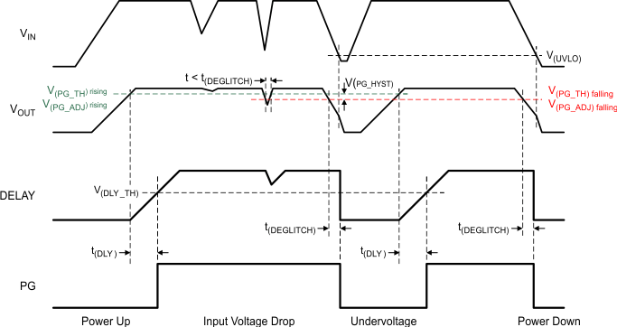
Adjustable Power-Good Delay Timer (DELAY)

The power-good delay period is a function of the external capacitor on the DELAY pin. The adjustable delay configures the amount of time required before the PG pin becomes high. This delay is configured by connecting an external capacitor from this pin to GND. Figure 7-2 shows the typical timing diagram for the power-good delay pin. If the DELAY pin is left floating, the power-good delay is t(DLY_FIX). For more information on how to program the PG delay, see the Section 8.1.7.1 section.
GUID-7BD43AF0-322D-495F-8446-DCBC72783815-low.gif
V(PG_TH) falling = V(PG_TH) rising – V(PG_HYST)..
Figure 7-2 Typical Power-Good Timing Diagram