ZHCSGL0A April 2017 – August 2017 TPS7H1101A-SP
PRODUCTION DATA.
6 Specifications
6.1 Absolute Maximum Ratings
over operating free-air temperature range (unless otherwise noted) (1)| MIN | MAX | UNIT | ||
|---|---|---|---|---|
| Input voltage | VIN, PG | –0.3 | 7.5 | V |
| FB, COMP, PCL, CS, EN | –0.3 | VIN + 0.3 | ||
| Output voltage | VOUT, SS | –0.3 | 7.5 | V |
| PG terminal sink current | 0.001 | 5 | mA | |
| Maximum operating junction temperature, TJ | –55 | 150 | °C | |
| Storage temperature, Tstg | –55 | 150 | °C | |
(1) Stresses beyond those listed under Absolute Maximum Ratings may cause permanent damage to the device. These are stress ratings only, which do not imply functional operation of the device at these or any other conditions beyond those indicated under Recommended Operating Conditions. Exposure to absolute-maximum-rated conditions for extended periods may affect device reliability.
6.2 ESD Ratings
| VALUE | UNIT | |||
|---|---|---|---|---|
| V(ESD) | Electrostatic discharge | Human-body model (HBM), per ANSI/ESDA/JEDEC JS-001, all pins(1) | ±2000 | V |
| Charged-device model (CDM), per JEDEC specification JESD22-C101, all pins(2) | ±1000 | |||
(1) JEDEC document JEP155 states that 500-V HBM allows safe manufacturing with a standard ESD control process.
(2) JEDEC document JEP157 states that 250-V CDM allows safe manufacturing with a standard ESD control process.
6.3 Recommended Operating Conditions
over operating free-air temperature range (unless otherwise noted)| MIN | NOM | MAX | UNIT | |||
|---|---|---|---|---|---|---|
| TJ | Operating junction temperature | –55 | 125 | °C | ||
6.4 Thermal Information
| THERMAL METRIC(1)(2) | TPS7H1101A-SP | UNIT | |
|---|---|---|---|
| HKR (CFP) | |||
| 16 PINS | |||
| RθJC(bot) | Junction-to-case (bottom) thermal resistance | 0.6 | °C/W |
(1) Do not allow package body temperature to exceed 265°C at any time or permanent damage may result.
(2) Maximum power dissipation may be limited by overcurrent protection.
6.5 Electrical Characteristics
1.5 V ≤ VIN ≤ 7 V, VOUT(target) = VIN – 0.35 V, IOUT = 10 mA, VEN = 1.1 V, COUT = 22 µF, PG terminal pulled up to VIN with 50 kΩ, over operating temperature range (TJ = –55°C to 125°C), unless otherwise noted. Typical values are at TJ = 25°C.| PARAMETER | TEST CONDITIONS | MIN | TYP | MAX | UNIT | ||
|---|---|---|---|---|---|---|---|
| VIN | Input voltage range | 1.5 | 7 | V | |||
| VFB | Feedback terminal voltage(2) | 0 A ≤ IOUT ≤ 3 A, 1.5 V ≤ VIN ≤ 7 V | 0.594 | 0.605 | 0.616 | V | |
| VOUT | Output voltage range | 0.8 | VIN | V | |||
| Output voltage accuracy(2) | 0 A ≤ IOUT ≤ 3 A, 1.5 V ≤ VIN ≤ 7 V, VOUT = 0.8 V, 1.2 V, 1.8 V, 6.65 V |
–2% | 2% | ||||
| ΔVOUT%/ ΔVIN |
Line regulation | 1.5 V ≤ VIN ≤ 7 V | –0.07 | 0.01 | 0.07 | %/V | |
| ΔVOUT%/ ΔIOUT |
Load regulation | 0.8 V ≤ VOUT ≤ 6.65 V, 0 ≤ ILoad ≤ 3 A | 0.08 | %/A | |||
| ΔVOUT | DC input line regulation | 1.5 V ≤ VIN ≤ 7 V, VOUT = 0.8 V, 1.2 V, 1.8 V, IOUT = 10 mA, TJ = –55°C(1) |
0.5 | 3 | mV | ||
| 1.5 V ≤ VIN ≤ 7 V, VOUT = 0.8 V, 1.2 V, 1.8 V, IOUT = 10 mA, TJ = 25°C(1) |
0.2 | 0.6 | |||||
| 1.5 V ≤ VIN ≤ 7 V, VOUT = 0.8 V, 1.2 V, 1.8 V, IOUT = 10 mA, TJ = 125°C(1) |
0.2 | 1 | |||||
| ΔVO | DC output load regulation(3) | VOUT = 0.8 V, 0 ≤ ILoad ≤ 1 A, TJ = –55°C(1) | 0.4 | 1 | mV | ||
| VOUT = 0.8 V, 0 ≤ ILoad ≤ 1 A, TJ = 25°C(1) | 0.6 | 1.1 | |||||
| VOUT = 0.8 V, 0 ≤ ILoad ≤ 1 A, TJ = 125°C(1) | 0.8 | 1.3 | |||||
| VOUT = 0.8 V, 0 ≤ ILoad ≤ 2 A, TJ = –55°C(1) | 0.8 | 1.8 | |||||
| VOUT = 0.8 V, 0 ≤ ILoad ≤ 2 A, TJ = 25°C(1) | 1.3 | 1.8 | |||||
| VOUT = 0.8 V, 0 ≤ ILoad ≤ 2 A, TJ = 125°C(1) | 1.6 | 2.4 | |||||
| VOUT = 0.8 V, 0 ≤ ILoad ≤ 3 A, TJ = –55°C(1) | 1.1 | 1.9 | |||||
| VOUT = 0.8 V, 0 ≤ ILoad ≤ 3 A, TJ = 25°C(1) | 1.9 | 2.6 | |||||
| VOUT = 0.8 V, 0 ≤ ILoad ≤ 3 A, TJ = 125°C(1) | 2.5 | 3.4 | |||||
| VOUT = 1.2 V, 0 ≤ ILoad ≤ 1 A, TJ = –55°C(1) | 0.3 | 1.2 | |||||
| VOUT = 1.2 V, 0 ≤ ILoad ≤ 1 A, TJ = 25°C(1) | 0.5 | 1.3 | |||||
| VOUT = 1.2 V, 0 ≤ ILoad ≤ 1 A, TJ = 125°C(1) | 0.6 | 1.3 | |||||
| VOUT = 1.2 V, 0 ≤ ILoad ≤ 2 A, TJ = –55°C(1) | 0.8 | 1.6 | |||||
| VOUT = 1.2 V, 0 ≤ ILoad ≤ 2 A, TJ = 25°C(1) | 1.1 | 2.1 | |||||
| VOUT = 1.2 V, 0 ≤ ILoad ≤ 2 A, TJ = 125°C(1) | 1.5 | 2.1 | |||||
| VOUT = 1.2 V, 0 ≤ ILoad ≤ 3 A, TJ = –55°C(1) | 1 | 1.7 | |||||
| VOUT = 1.2 V, 0 ≤ ILoad ≤ 3 A, TJ = 25°C(1) | 1.1 | 2.4 | |||||
| VOUT = 1.2 V, 0 ≤ ILoad ≤ 3 A, TJ = 125°C(1) | 2.2 | 3.5 | |||||
| VOUT = 1.8 V, 0 ≤ ILoad ≤ 1 A, TJ = –55°C(1) | 0.1 | 0.9 | |||||
| VOUT = 1.8 V, 0 ≤ ILoad ≤ 1 A, TJ = 25°C(1) | 0.3 | 0.9 | |||||
| VOUT = 1.8 V, 0 ≤ ILoad ≤ 1 A, TJ = 125°C(1) | 0.4 | 1.2 | |||||
| VOUT = 1.8 V, 0 ≤ ILoad ≤ 2 A, TJ = –55°C(1) | 1.4 | 2.4 | |||||
| VOUT = 1.8 V, 0 ≤ ILoad ≤ 2 A, TJ = 25°C(1) | 0.7 | 1.4 | |||||
| VOUT = 1.8 V, 0 ≤ ILoad ≤ 2 A, TJ = 125°C(1) | 0.6 | 1.9 | |||||
| VOUT = 1.8 V, 0 ≤ ILoad ≤ 3 A, TJ = –55°C(1) | 2.5 | 3.9 | |||||
| VOUT = 1.8 V, 0 ≤ ILoad ≤ 3 A, TJ = 25°C(1) | 1.2 | 2.1 | |||||
| VOUT = 1.8 V, 0 ≤ ILoad ≤ 3 A, TJ = 125°C(1) | 1.2 | 2.5 | |||||
| VOUT = 6.65 V, 0 ≤ ILoad ≤ 1 A, TJ = –55°C(1) | 1.5 | 2.9 | |||||
| VOUT = 6.65 V, 0 ≤ ILoad ≤ 1 A, TJ = 25°C(1) | 0.4 | 2.6 | |||||
| VOUT = 6.65 V, 0 ≤ ILoad ≤ 1 A, TJ = 125°C(1) | 2.8 | 3.5 | |||||
| VOUT = 6.65 V, 0 ≤ ILoad ≤ 2 A, TJ = –55°C(1) | 3.5 | 5.9 | |||||
| VOUT = 6.65 V, 0 ≤ ILoad ≤ 2 A, TJ = 25°C(1) | 1.1 | 4.7 | |||||
| VOUT = 6.65 V, 0 ≤ ILoad ≤ 2 A, TJ = 125°C(1) | 5.8 | 8 | |||||
| VOUT = 6.65 V, 0 ≤ ILoad ≤ 3 A, TJ = –55°C(1) | 5.6 | 9.3 | |||||
| VOUT = 6.65 V, 0 ≤ ILoad ≤ 3 A, TJ = 25°C(1) | 3.7 | 8 | |||||
| VOUT = 6.65 V, 0 ≤ ILoad ≤ 3 A, TJ = 125°C(1) | 13 | 25 | |||||
| VDO | Dropout voltage(3) | IOUT = 3 A, VOUT = 1.3 V, VIN = VOUT + VDO | 210 | 335 | mV | ||
| ICL | Programmable output current limit range | VIN = 1.5 V, VOUT = 1.2 V, PCL resistance = 47 kΩ |
500 | 750 | mA | ||
| VIN = 1.5 V, VOUT = 1.2 V, PCL resistance varies |
200 | 3500(5) | |||||
| VCS | Operating voltage range at CS | 0.3 | VIN | V | |||
| CSR | Current sense ratio | ILOAD / ICS, VIN = 2.3 V, VOUT = 1.9 V | 47394 | 47500 | 56000 | A/A | |
| IGND | GND terminal current | VIN = 1.5 V, VOUT = 1.2 V, IOUT = 2 A | 10 | 16 | mA | ||
| IQ | Quiescent current (no load) | VIN = VOUT + 0.5 V, IOUT = 0 A | 7 | 10 | mA | ||
| ISHDN | Shutdown current | 1.5 V ≤ VIN ≤ 7 V, pre and post 100 krads (Si), TJ = 25°C(4) | 26 | 230 | µA | ||
| ISNS, IFB | FB/SNS terminal current | VIN = 7 V, VOUT = 6.65 V | 1 | 5 | nA | ||
| IEN | EN terminal input current | VIN = 7 V, VEN = 7 V, VOUT = 6.65 V | 20 | 150 | nA | ||
| VILEN | EN terminal input low (disable) | 1.5 V < VIN < 7 V | 0.55 | V | |||
| VIHEN | EN terminal input high (enable) | 1.5 V < VIN < 7 V | VIN – 0.7 | V | |||
| Eprop Dly | Enable terminal propagation delay | VIN = 2.2 V, EN rise to IOUTrise | 650 | 1000 | µs | ||
| TEN | Enable terminal turn-on delay | VIN = 2.2 V, VOUT = 1.8 V, ILOAD = 1 A, COUT = 220 µF, CSS = 2 nF |
1.4 | 1.6 | ms | ||
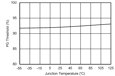
| VTHPG | PG threshold | No load, 0.8 V ≤ VOUT ≤ 6.65 V | 86% | 90% | |||
| VTHPGHYS | PG hysteresis | 1.5 V ≤ VIN ≤ 7 V | 2% | ||||
| VOLPG | PG terminal output low | IPG = 0 mA to –1 mA | 120 | 300 | mV | ||
| ILKGPG | PG terminal leakage current | VOUT > VTHPG, VPG = 1.2 V | 0.2 | 1.5 | µA | ||
| VOUT > VTHPG, VPG = 7 V | 0.5 | 2.5 | |||||
| ISS | SS terminal charge current | VIN = 1.5 V to 7 V | 2.5 | 3.5 | µA | ||
| ISSdisb | SS terminal disable current | VIN = 1.5 V to 7 V | 5 | 10 | µA | ||
| VSS | SS terminal voltage (device enabled)(6) | VIN = 1.5 V to 7 V | 1.232 | V | |||
| VSSdisb | SS terminal low-level input voltage to disable device | VIN = 1.5 V to 7 V | 0.4 | V | |||
| PSRR | Power-supply rejection ratio | VIN = 2.5 V, VOUT = 1.8 V, COUT = 220 µF |
1 kHz | 48 | dB | ||
| 100 kHz | 25 | ||||||
| VN | Output noise voltage | BW = 10 Hz to 100 kHz, IOUT = 3 A, VIN = 2 V, VOUT = 1.8 V |
20.33 | µVRMS | |||
| TSD | Thermal shutdown temperature | 185 | °C | ||||
(1) Line and load regulations done under pulse condition for t < 10 ms.
(2) The output voltage accuracy of condition at IOUT = 2 A and IOUT = 3 A is specified by characterization, but not production tested.
(3) The parameter is specified to the limit in characterization, but not production tested.
(4) This maximum limit applies to SMD 5962R13202 post 100-krads (Si) test at 25°C.
(5) The maximum limit of the ICLparameter is specified to the limit in characterization, but not production tested.
(6) Any external pullup voltage should not exceed 1.188 V.
6.6 Typical Characteristics
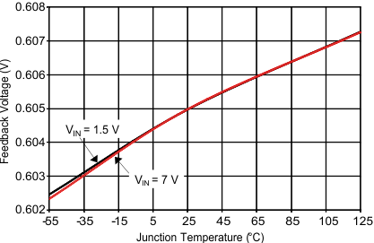
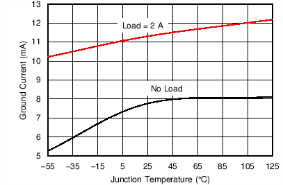
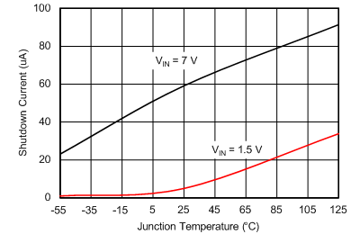
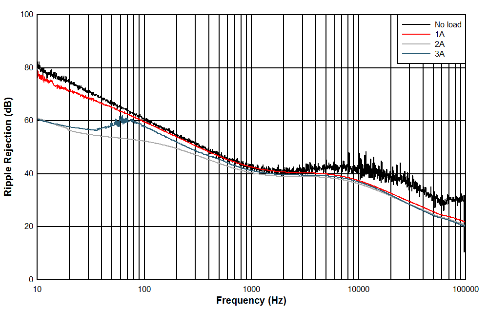
| VIN = 2.5 V | VOUT = 1.8 V | |
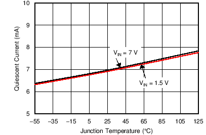
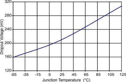
| VOUT = 1.8 V | Load = 3 A | |
