ZHCSGD1 June 2017 TPS82140
PRODUCTION DATA.
- 1 特性
- 2 应用
- 3 说明
- 4 修订历史记录
- 5 Pin Configuration and Functions
- 6 Specifications
- 7 Detailed Description
- 8 Application and Implementation
- 9 Power Supply Recommendations
- 10Layout
- 11器件和文档支持
- 12机械、封装和可订购信息
10 Layout
10.1 Layout Guidelines
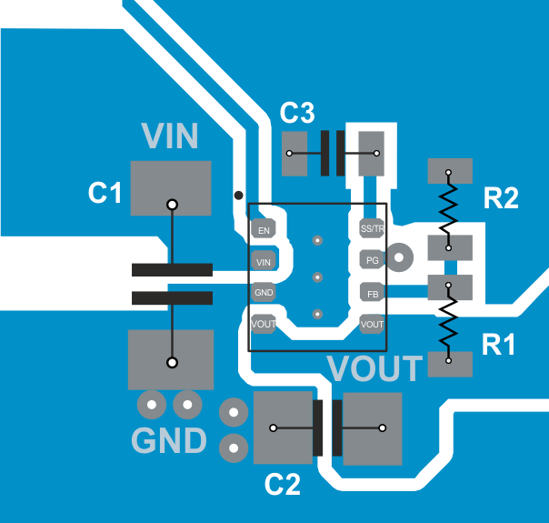
- TI recommends placing all components as close as possible to the IC. The input capacitor placement specifically, must be closest to the VIN and GND pins of the device.
- Use wide and short traces for the main current paths to reduce the parasitic inductance and resistance.
- To enhance heat dissipation of the device, the exposed thermal pad should be connected to bottom or internal layer ground planes using vias.
- Refer to Figure 31 for an example of component placement, routing and thermal design.
10.2 Layout Example
space
space
 Figure 31. TPS82140 PCB Layout
10.3 Thermal Consideration
The output current of the TPS82140 needs to be derated when the device operates in a high ambient temperature or delivers high output power. The amount of current derating is dependent upon the input voltage, output power, PCB layout design and environmental thermal condition. Care should especially be taken in applications where the localized PCB temperature exceeds 65°C.
The TPS82140 module temperature must be kept less than the maximum rating of 125°C. Three basic approaches for enhancing thermal performance are below:
- Improve the power dissipation capability of the PCB design.
- Improve the thermal coupling of the TPS82140 to the PCB.
- Introduce airflow into the system.
To estimate approximate module temperature of TPS82140, apply the typical efficiency stated in this datasheet to the desired application condition to find the module's power dissipation. Then calculate the module temperature rise by multiplying the power dissipation by its thermal resistance. For more details on how to use the thermal parameters in real applications, see the application notes: SZZA017 and SPRA953.