SLVSBR0C October 2014 – June 2015 TPS8268090 , TPS8268105 , TPS8268120 , TPS8268150 , TPS8268180
PRODUCTION DATA.
- 1 Features
- 2 Applications
- 3 Description
- 4 Revision History
- 5 Device Comparison Table
- 6 Pin Configuration and Functions
- 7 Specifications
- 8 Detailed Description
- 9 Application and Implementation
- 10Power Supply Recommendations
- 11Layout
- 12Device and Documentation Support
- 13Mechanical, Packaging, and Orderable Information
11 Layout
11.1 Layout Guidelines
TPS8268x allows the design of a power supply with small solution size. In order to properly dissipate the heat, wide copper traces for the power connections should be used to distribute the heat across the PCB. If possible, a GND plane should be used as it provides a low impedance connection as well as serves as a heat sink.
In making the pad size for the SiP LGA balls, it is recommended that the layout use a non-solder-mask defined (NSMD) land. With this method, the solder mask opening is made larger than the desired land area, and the opening size is defined by the copper pad width. Figure 44 shows the appropriate diameters for a MicroSiPTM layout.
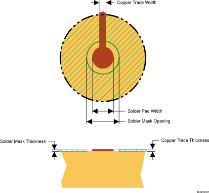 Figure 44. Recommended Land Pattern Image and Dimensions
| SOLDER PAD DEFINITIONS(1)(2)(3)(4) | COPPER PAD | SOLDER MASK (5)
OPENING |
COPPER THICKNESS | STENCIL (6)
OPENING |
STENCIL THICKNESS |
|---|---|---|---|---|---|
| Non-solder-mask defined (NSMD) | 0.30mm | 0.360mm | 1oz max (0.032mm) | 0.34mm diameter | 0.1mm thick |
11.2 Layout Example
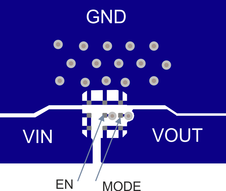 Figure 45. Recommended PCB Layout
11.3 Surface Mount Information
The TPS8268x MicroSiP™ DC/DC converter uses an open frame construction that is designed for a fully automated assembly process and that features a large surface area for pick and place operations. See the "Pick Area" in the package drawings.
Package height and weight have been kept to a minimum to allow the MicroSiP™ device to be handled similarly to a 0805 component.
See JEDEC/IPC standard J-STD-20b for reflow recommendations.
11.4 Thermal and Reliability Information
The TPS8268x´s output current may need to be de-rated if it is required to operate in a high ambient temperature or deliver a large amount of continuous power. The amount of current de-rating is dependent upon the input voltage, output power and environmental thermal conditions. Care should especially be taken in applications where the localized PCB temperature exceeds 65°C.
The TPS8268x die and inductor temperature should be kept lower than the maximum rating of 125°C, so care should be taken in the circuit layout to ensure good heat sinking. Sufficient cooling should be provided to ensure reliable operation.
Three basic approaches for enhancing thermal performance are listed below:
- Improve the power dissipation capability of the PCB design.
- Improve the thermal coupling of the component to the PCB.
- Introduce airflow into the system.
To estimate the junction temperature, approximate the power dissipation within the TPS8268x by applying the typical efficiency stated in this datasheet to the desired output power; or, by taking an actual power measurement. Then, calculate the internal temperature rise of the TPS8268x above the surface of the printed circuit board by multiplying the TPS8268x´s power dissipation by its thermal resistance.
The thermal resistance numbers listed in the Thermal Information table are based on modeling the MicroSiP™ package mounted on a high-K test board specified per the JEDEC standard. For increased accuracy and fidelity to the actual application, it is recommended to run a thermal image analysis of the actual system.
Thermal measurements have been taken on the EVM to give a guideline on what temperature can be expected when the device is operated in free air at 25°C ambient under a certain load. The temperatures have been checked at 4 different spots as listed below:
- Spot1: temperature of the input capacitor
- Spot2: temperature of the output capacitor
- Spot3: temperature of the inductor
- Spot4: temperature on the main pcb next to the module
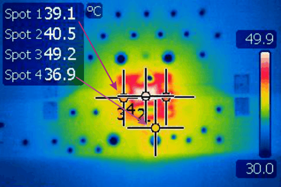 Figure 46. VIN= 5V, VOUT=1.05V, IOUT= 1A
388mW Power Dissipation
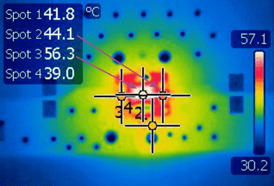 Figure 47. VIN= 5V, VOUT= 1.05V, IOUT= 1.2A
466mW Power Dissipation
The TPS8268x contains a thermal shutdown that inhibits switching at high junction temperatures. The activation threshold of this function, however, is above 125°C to avoid interfering with normal operation. Thus, prolonged or repetitive operation under a condition in which the thermal shutdown activates necessarily means that the components internal to the MicroSiP™ package are subjected to high temperatures for prolonged or repetitive intervals, which may decrease the reliability of the device.
MLCC capacitor reliability/lifetime depends on temperature and applied voltage. At higher temperatures, MLCC capacitors are subject to stronger stress. On the basis of frequently evaluated failure rates determined with standardized test conditions, the reliability of all MLCC capacitors can be calculated for their actual operating temperature and voltage.
Failures caused by systematic degradation are described by the Arrhenius model. The most critical parameter (IR) is the Insulation Resistance (i.e. leakage current). The drop of IR below a lower limit (e.g. 1 MΩ) is used as the failure criterion. See Figure 48 and Figure 49. Note that the wear-out mechanisms occurring in the MLCC capacitors are not reversible but cumulative over time.
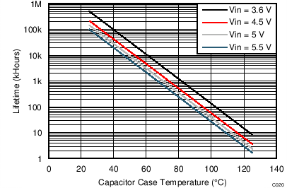 Figure 48. Input Capacitor Lifetime
| Input Capacitor Lifetime
vs Temperature and Voltage |
Output Capacitor Lifetime
vs Temperature and Voltage |
|
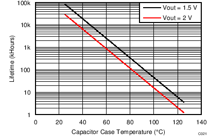 Figure 49. Output Capacitor Lifetime