ZHCSCJ5A June 2014 – June 2014 TPS82740A , TPS82740B
PRODUCTION DATA.
- 1 特性
- 2 应用范围
- 3 说明
- 4 典型应用
- 5 修订历史记录
- 6 Device Comparison Table
- 7 Pin Configuration and Functions
- 8 Specifications
- 9 Parameter Measurement Information
- 10Detailed Description
- 11Application and Implementation
- 12Power Supply Recommendations
- 13Layout
- 14器件和文档支持
- 15机械封装和可订购信息
11 Application and Implementation
11.1 Application Information
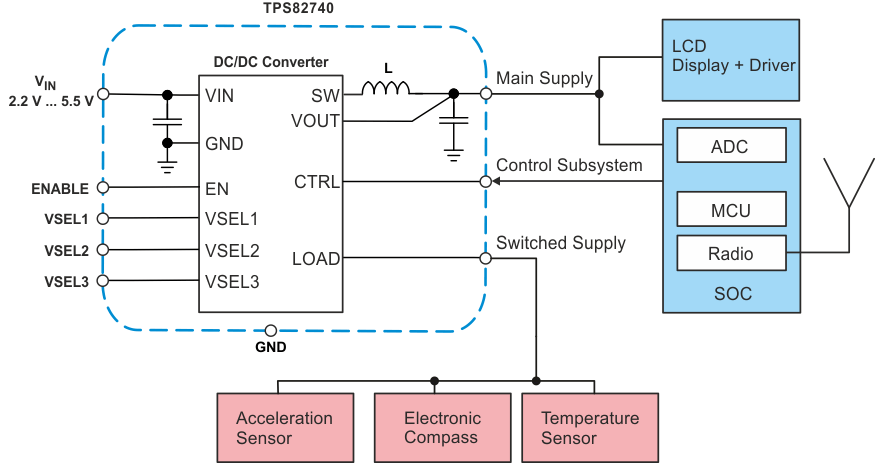
The device is designed to operate from an input voltage supply range between 2.2V and 5.5V with a maximum output current of 200mA. Once the input voltage comes close to the output voltage, the DC/DC converter stops switching and enters 100% duty cycle operation. The integrated slew rate controlled load switch can distribute the selected output voltage to a temporarily used sub-system. The TPS82740 module operates in PWM mode for medium and high load conditions and in power save mode at light load currents.
At high load currents, the converter operates in quasi fixed frequency PWM mode operation. The switching frequency is up to 1.7MHz with a controlled frequency variation depending on the input voltage. If the load current decreases, the converter seamlessly enters Power Save Mode by varying the switching frequency linearly to maintain high efficiency over the full load current range. At very light load conditions the device generates a single switching pulse to ramp up the inductor current and recharge the output capacitor, followed by a sleep period where most of the internal circuits are shutdown to achieve 360nA quiescent current consumption.
11.2 Typical Application
 Example of Implementation in a SOC Based System
11.2.1 Design Requirements
TPS82740 is a complete step-down converter module including all passive components (inductor, input and output capacitor). For most applications no additional input / output capacitors are required. Use the following typical application design procedure to select additional external components in case further performance improvement of the module is desired.
11.2.2 Detailed Design Procedure
11.2.2.1 Input Capacitor Selection
For most applications, the integrated input capacitor at the VIN pin is sufficient.
TPS82740 uses a tiny ceramic input capacitor. When a ceramic capacitor is combined with trace or cable inductance, such as that from a wall adapter, a load step at the output can induce ringing at the VIN pin. This ringing can couple to the output and be mistaken as loop instability or can even damage the module. In this circumstance, additional ceramic 'bulk" capacitance, such as electrolytic or tantalum, should be placed between the input of the module and the power source lead to reduce ringing that occurs between the inductance of the power source leads and the module.
11.2.2.1.1 Input Buffer Capacitor Selection
In addition to the small ceramic input capacitor a larger buffer capacitor CBuf is recommended to reduce voltage drops and ripple voltage. When using battery chemistries like Li-SOCl2, Li-SO2, Li-MnO2, the impedance of the battery has to be considered. These battery types tend to increase their impedance depending on discharge status and often can support output currents of only a few mA. Therefore a buffer capacitor is recommended to stabilize the battery voltage during DC/DC operations e.g. for a RF transmission. A voltage drop on the input of the TPS82740 during DC/DC operation impacts the advantage of the step down conversion for system power reduction. Furthermore the voltage drops can fall below the minimum recommended operating voltage of the device and leads to an early system cut off. Both effects reduce the battery life time. To achieve best performance and to extract the most energy out of the battery a good procedure is to select the buffer capacitor value for an voltage drop below 50mVpp during DC/DC operation. The capacitor value strongly depends on the used battery type, as well the current consumption during a RF transmission as well the duration of the transmission.
11.2.2.2 Output Capacitor Selection
For most applications, the integrated output capacitor at the VOUT pin is sufficient.
In order to further reduce the output voltage ripple and improve the load transient performance an additional external output capacitance may be used. For most applications an additional 4.7µF or 10µF capacitor will be sufficient. Care should be taken that the total effective capacitance present at the output does not exceed 10µF in order to guarantee loop stability. Ceramic capacitors with low ESR values have the lowest output voltage ripple and are recommended.
At the LOAD output pin, no additional output capacitor is required. For applications demanding external capacitance connected to the LOAD pin, the total capacitance should not exceed 10µF.
11.2.3 Application Curves
 Figure 41. TPS82740B Device Enable and Start up
 Figure 43. TPS82740B VOUT Ramp with activated LOAD Switch
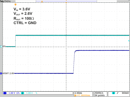
 Figure 42. TPS82740B VOUT Ramp after Enable
 Figure 44. TPS82740A Dynamic Output Voltage Scaling: VOUT = 1.8V / 2.5V