ZHCSL07C September 2019 – August 2021 TPS8802
PRODUCTION DATA
- 1 特性
- 2 应用
- 3 说明
- 4 Revision History
- 5 Pin Configuration and Functions
- 6 Specifications
- 7 Typical Characteristics
-
8 Detailed Description
- 8.1 Overview
- 8.2 Functional Block Diagram
- 8.3
Feature Description
- 8.3.1 System Power-up
- 8.3.2 LDO Regulators
- 8.3.3 Photo Chamber AFE
- 8.3.4 LED Driver
- 8.3.5 Carbon Monoxide Sensor AFE
- 8.3.6 Boost Converter
- 8.3.7 Interconnect Driver
- 8.3.8 Piezoelectric Horn Driver
- 8.3.9 Battery Test
- 8.3.10 AMUX
- 8.3.11 Analog Bias Block and 8 MHz Oscillator
- 8.3.12 Interrupt Signal Alerts
- 8.4 Device Functional Modes
- 8.5 Programming
- 8.6
Register Maps
- 8.6.1 REVID Register (Offset = 0h) [reset = 0h]
- 8.6.2 STATUS1 Register (Offset = 1h) [reset = 0h]
- 8.6.3 STATUS2 Register (Offset = 2h) [reset = 0h]
- 8.6.4 MASK Register (Offset = 3h) [reset = 0h]
- 8.6.5 CONFIG1 Register (Offset = 4h) [reset = 20h]
- 8.6.6 CONFIG2 Register (Offset = 5h) [reset = 2h]
- 8.6.7 ENABLE1 Register (Offset = 6h) [reset = 10h]
- 8.6.8 ENABLE2 Register (Offset = 7h) [reset = 0h]
- 8.6.9 CONTROL Register (Offset = 8h) [reset = 0h]
- 8.6.10 SLPTMR1 Register (Offset = 9h) [reset = 0h]
- 8.6.11 SLPTMR2 Register (Offset = Ah) [reset = 0h]
- 8.6.12 GPIO_AMUX Register (Offset = Bh) [reset = 0h]
- 8.6.13 CO_BATTEST Register (Offset = Ch) [reset = 0h]
- 8.6.14 CO Register (Offset = Dh) [reset = 0h]
- 8.6.15 VBOOST Register (Offset = Eh) [reset = F2h]
- 8.6.16 LEDLDO Register (Offset = Fh) [reset = 0h]
- 8.6.17 PH_CTRL Register (Offset = 10h) [reset = 0h]
- 8.6.18 LED_DAC_A Register (Offset = 11h) [reset = 0h]
- 8.6.19 LED_DAC_B Register (Offset = 12h) [reset = 0h]
- 9 Application and Implementation
- 10Power Supply Recommendations
- 11Layout
- 12Device and Documentation Support
- 13Mechanical, Packaging, and Orderable Information
8.3.1 System Power-up
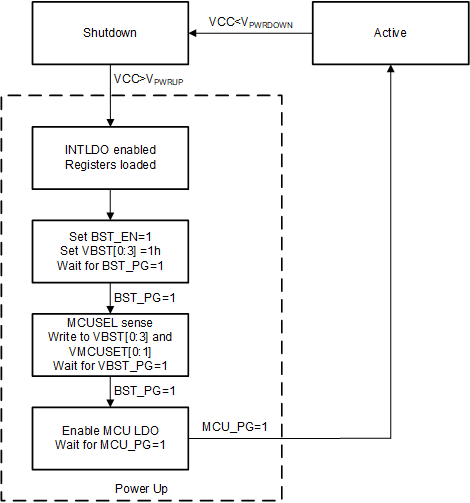
 Figure 8-1 Power-up State Diagram
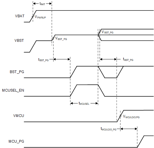
The TPS8802 can power-up from a battery above 2V connected to the input of the boost converter. This is achieved with an automatic power-up sequence. When the VCC voltage exceeds the VPWRUP threshold, the device initializes for 6 ms. After the initialization, the boost converter is enabled and set to 3.8V. In a 3V battery powered system where VCC is connected to VBST, this raises the VCC and VBST voltage to provide power to the internal digital and analog blocks. The VBST voltage must exceed the power-good threshold for the 3.8V setting (typically 95% of its target voltage) for the power-up sequence to proceed. The MCUSEL pin is then sensed for 2 ms to determine the MCULDO voltage and program the VMCUSET and VBST register accordingly. Table 8-1 indicates the VMCU and VBST setting for each MCUSEL configuration. After VBST reaches its power-good threshold again, the MCULDO is enabled and the system waits for VMCU to reach its power-good threshold (typically 85% of its target voltage). The device enters its active state after VMCU reaches its power-good threshold. This sequence of events is outlined in Figure 8-1 and Figure 8-2.
If the boost converter is not being used, the same power-up sequence occurs, but the boost converter is not able to raise the voltage higher than what is supplied. The minimum VCC and VBST voltage depends on the VMCU voltage. If the MCUSEL pin sets VMCU to 1.5 V, 1.8 V, or 2.5 V, supply over 3.8V on VBST. If the MCUSEL pin sets VMCU to 3.3 V, supply over 4.7 V on VBST. If VMCU is set to 1.5 V, 1.8 V, or 2.5 V, provide over 2.6 V to VCC for power-up. If VMCU is set to 3.3 V, provide over 3.6 V to VCC for power-up. Higher VCC voltage may required depending on the VMCU load current.
| MCUSEL Connection | VMCU (V) | VBST (V) |
|---|---|---|
| 620-Ω to GND | 1.5 | 2.7 |
| Short to GND | 1.8 | 2.7 |
| Short to VINT | 2.5 | 3.8 |
| 330-pF to GND | 3.3 | 4.7 |
 Figure 8-2 Power-up Timing Diagram