ZHCSL07C September 2019 – August 2021 TPS8802
PRODUCTION DATA
- 1 特性
- 2 应用
- 3 说明
- 4 Revision History
- 5 Pin Configuration and Functions
- 6 Specifications
- 7 Typical Characteristics
-
8 Detailed Description
- 8.1 Overview
- 8.2 Functional Block Diagram
- 8.3
Feature Description
- 8.3.1 System Power-up
- 8.3.2 LDO Regulators
- 8.3.3 Photo Chamber AFE
- 8.3.4 LED Driver
- 8.3.5 Carbon Monoxide Sensor AFE
- 8.3.6 Boost Converter
- 8.3.7 Interconnect Driver
- 8.3.8 Piezoelectric Horn Driver
- 8.3.9 Battery Test
- 8.3.10 AMUX
- 8.3.11 Analog Bias Block and 8 MHz Oscillator
- 8.3.12 Interrupt Signal Alerts
- 8.4 Device Functional Modes
- 8.5 Programming
- 8.6
Register Maps
- 8.6.1 REVID Register (Offset = 0h) [reset = 0h]
- 8.6.2 STATUS1 Register (Offset = 1h) [reset = 0h]
- 8.6.3 STATUS2 Register (Offset = 2h) [reset = 0h]
- 8.6.4 MASK Register (Offset = 3h) [reset = 0h]
- 8.6.5 CONFIG1 Register (Offset = 4h) [reset = 20h]
- 8.6.6 CONFIG2 Register (Offset = 5h) [reset = 2h]
- 8.6.7 ENABLE1 Register (Offset = 6h) [reset = 10h]
- 8.6.8 ENABLE2 Register (Offset = 7h) [reset = 0h]
- 8.6.9 CONTROL Register (Offset = 8h) [reset = 0h]
- 8.6.10 SLPTMR1 Register (Offset = 9h) [reset = 0h]
- 8.6.11 SLPTMR2 Register (Offset = Ah) [reset = 0h]
- 8.6.12 GPIO_AMUX Register (Offset = Bh) [reset = 0h]
- 8.6.13 CO_BATTEST Register (Offset = Ch) [reset = 0h]
- 8.6.14 CO Register (Offset = Dh) [reset = 0h]
- 8.6.15 VBOOST Register (Offset = Eh) [reset = F2h]
- 8.6.16 LEDLDO Register (Offset = Fh) [reset = 0h]
- 8.6.17 PH_CTRL Register (Offset = 10h) [reset = 0h]
- 8.6.18 LED_DAC_A Register (Offset = 11h) [reset = 0h]
- 8.6.19 LED_DAC_B Register (Offset = 12h) [reset = 0h]
- 9 Application and Implementation
- 10Power Supply Recommendations
- 11Layout
- 12Device and Documentation Support
- 13Mechanical, Packaging, and Orderable Information
8.3.8.2 Two-Terminal Piezo
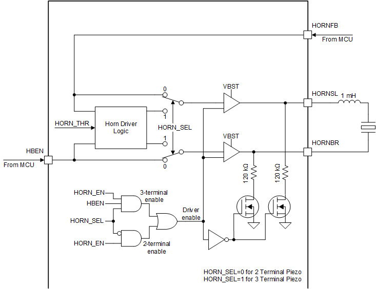
 Figure 8-10 Two-Terminal Piezoelectric Horn Driver Circuit
In the two-terminal mode, the piezo connects to the HORNSL and HORNBR terminals through an inductor. The HORNFB pin directly controls the HORNSL pin, and the HBEN pin directly controls the HORNBR pin. The two drivers are matched to minimize skew between the two outputs. The MCU sends a digital signal to control the driving voltage across the piezo. The signal can be a square wave of the oscillation frequency, a pulse width modulation (PWM) sine wave of the oscillation frequency, or a PWM arbitrary shape for voice applications. The inductor improves the rise time and fall time of the output and reduces power dissipation.