ZHCSL07C September 2019 – August 2021 TPS8802
PRODUCTION DATA
- 1 特性
- 2 应用
- 3 说明
- 4 Revision History
- 5 Pin Configuration and Functions
- 6 Specifications
- 7 Typical Characteristics
-
8 Detailed Description
- 8.1 Overview
- 8.2 Functional Block Diagram
- 8.3
Feature Description
- 8.3.1 System Power-up
- 8.3.2 LDO Regulators
- 8.3.3 Photo Chamber AFE
- 8.3.4 LED Driver
- 8.3.5 Carbon Monoxide Sensor AFE
- 8.3.6 Boost Converter
- 8.3.7 Interconnect Driver
- 8.3.8 Piezoelectric Horn Driver
- 8.3.9 Battery Test
- 8.3.10 AMUX
- 8.3.11 Analog Bias Block and 8 MHz Oscillator
- 8.3.12 Interrupt Signal Alerts
- 8.4 Device Functional Modes
- 8.5 Programming
- 8.6
Register Maps
- 8.6.1 REVID Register (Offset = 0h) [reset = 0h]
- 8.6.2 STATUS1 Register (Offset = 1h) [reset = 0h]
- 8.6.3 STATUS2 Register (Offset = 2h) [reset = 0h]
- 8.6.4 MASK Register (Offset = 3h) [reset = 0h]
- 8.6.5 CONFIG1 Register (Offset = 4h) [reset = 20h]
- 8.6.6 CONFIG2 Register (Offset = 5h) [reset = 2h]
- 8.6.7 ENABLE1 Register (Offset = 6h) [reset = 10h]
- 8.6.8 ENABLE2 Register (Offset = 7h) [reset = 0h]
- 8.6.9 CONTROL Register (Offset = 8h) [reset = 0h]
- 8.6.10 SLPTMR1 Register (Offset = 9h) [reset = 0h]
- 8.6.11 SLPTMR2 Register (Offset = Ah) [reset = 0h]
- 8.6.12 GPIO_AMUX Register (Offset = Bh) [reset = 0h]
- 8.6.13 CO_BATTEST Register (Offset = Ch) [reset = 0h]
- 8.6.14 CO Register (Offset = Dh) [reset = 0h]
- 8.6.15 VBOOST Register (Offset = Eh) [reset = F2h]
- 8.6.16 LEDLDO Register (Offset = Fh) [reset = 0h]
- 8.6.17 PH_CTRL Register (Offset = 10h) [reset = 0h]
- 8.6.18 LED_DAC_A Register (Offset = 11h) [reset = 0h]
- 8.6.19 LED_DAC_B Register (Offset = 12h) [reset = 0h]
- 9 Application and Implementation
- 10Power Supply Recommendations
- 11Layout
- 12Device and Documentation Support
- 13Mechanical, Packaging, and Orderable Information
8.3.3 Photo Chamber AFE
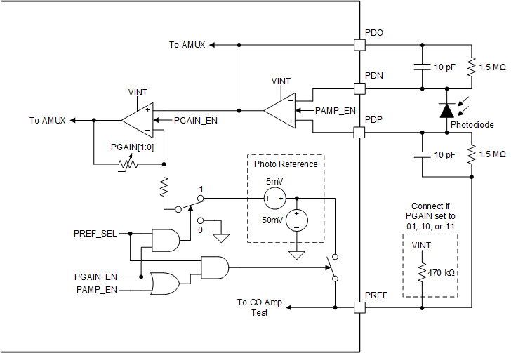
 Figure 8-3 Photo Amplifier Circuit
The TPS8802 photo amplifier connects to a photoelectric chamber photodiode and has two stages—an input stage and gain stage. When the photoelectric chamber LED is enabled, light scatters off smoke particles in the chamber into the photodiode, producing a signal proportional to the smoke concentration. The output of each photo amplifier stage is connected to the AMUX for ADC reading. This configuration provides high bandwidth and dynamic range for the photodiode signal chain as the gain stage is on-the-fly adjustable.