ZHCSLC6B May 2020 – January 2022 TPS92200
PRODUCTION DATA
- 1 特性
- 2 应用
- 3 说明
- 4 Revision History
- 5 Pin Configuration and Functions
- 6 Specifications
-
7 Detailed Description
- 7.1 Overview
- 7.2 Functional Block Diagram
- 7.3 Feature Description
- 7.4 Device Functional Modes
- 8 Application and Implementation
- 9 Power Supply Recommendations
- 10Layout
- 11Device and Documentation Support
- 12Mechanical, Packaging, and Orderable Information
6.7 Typical Characteristics
VIN = 12 V, unless otherwise specified.
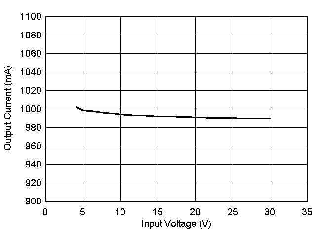 Figure 6-1 Output Current vs Input
Voltage
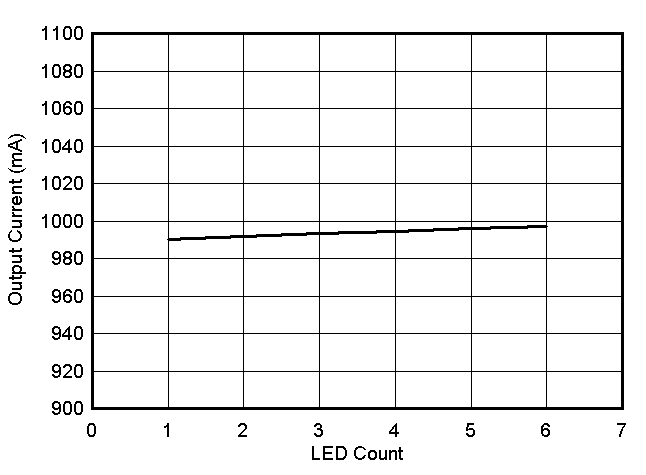 Figure 6-3 Output Current vs LED
Count
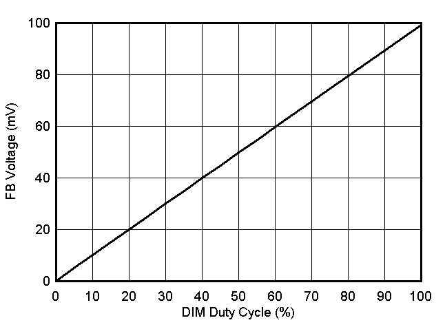 Figure 6-5 DIM Duty Cycle vs FB
Voltage in Analog Dimming (for TPS92200D2)
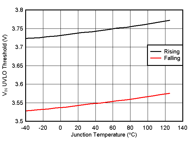 Figure 6-7 VIN UVLO Threshold vs
Junction Temperature
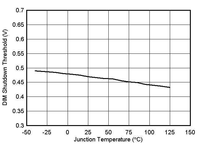 Figure 6-9 DIM Shutdown Threshold vs
Junction Temperature
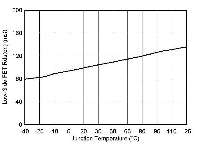 Figure 6-11 Low-Side FET On
Resistance vs Junction Temperature
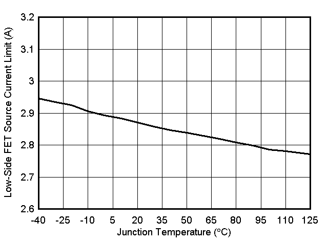 Figure 6-13 Low-Side FET Source
Current Limit vs Junction Temperature
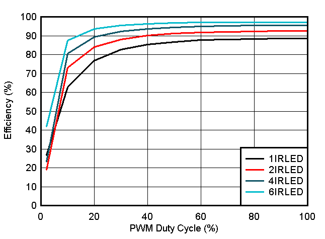 Figure 6-15 Efficiency at 1-A Output Current, 4.7-µH Inductor, 12-V Input Voltage
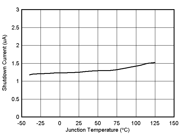 Figure 6-2 Shutdown Current vs
Junction Temperature
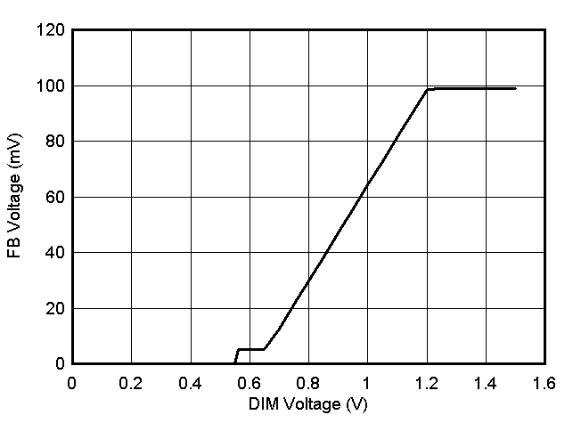 Figure 6-4 DIM Voltage vs FB Voltage
in Analog Dimming (for TPS92200D1)
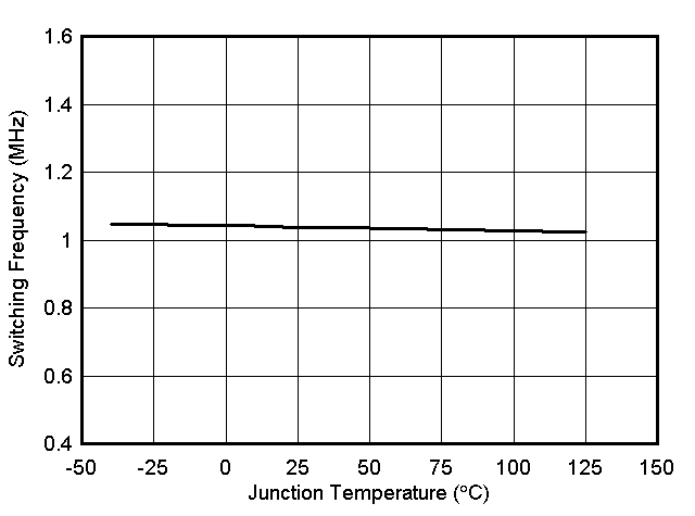 Figure 6-6 Switching Frequency vs
Junction Temperature
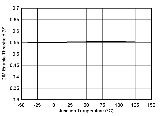 Figure 6-8 DIM Enable Threshold vs
Junction Temperature
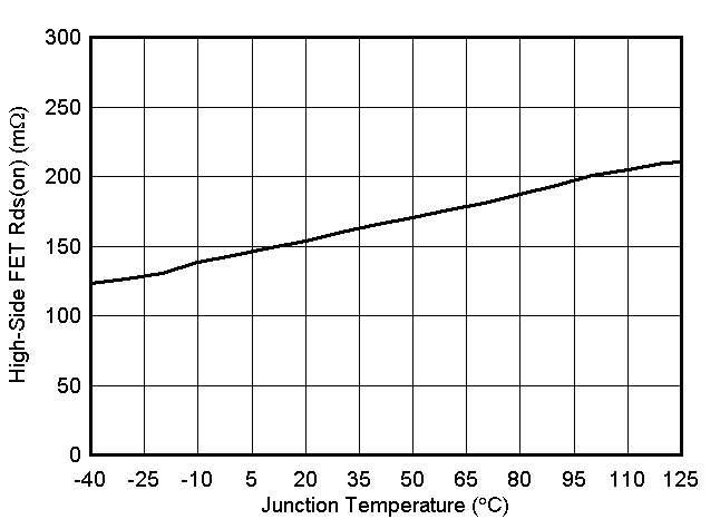 Figure 6-10 High-side FET On
Resistance vs Junction Temperature
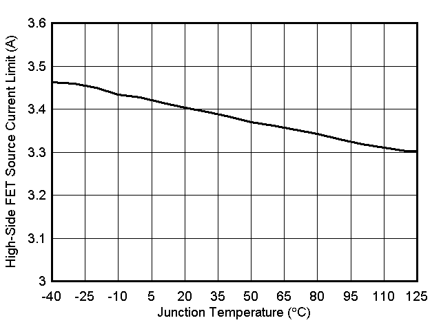 Figure 6-12 High-Side FET Source
Current Limit vs Junction Temperature
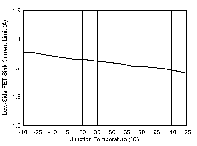 Figure 6-14 Low-Side FET Sink Current
Limit vs Junction Temperature
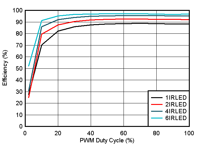 Figure 6-16 Efficiency at 1.5-A Output Current, 4.7-µH Inductor, 12-V Input Voltage