ZHCSDG5A February 2015 – March 2015 TPS92512 , TPS92512HV
PRODUCTION DATA.
- 1 特性
- 2 应用范围
- 3 说明
- 4 简化电路原理图
- 5 修订历史记录
- 6 Pin Configuration and Functions
- 7 Specifications
-
8 Detailed Description
- 8.1 Overview
- 8.2 Functional Block Diagram
- 8.3
Feature Description
- 8.3.1 Undervoltage Lockout and Low Power Shutdown (UVLO Pin)
- 8.3.2 Adjustable Switching Frequency (RT/CLK Pin)
- 8.3.3 Synchronizing the Switching Frequency to an External Clock (RT/CLK Pin)
- 8.3.4 Adjustable LED Current (IADJ and ISENSE Pins)
- 8.3.5 PWM Dimming (PDIM Pin)
- 8.3.6 External Compensation (COMP Pin)
- 8.3.7 Overcurrent Protection
- 8.3.8 Overtemperature Protection
- 8.4 Device Functional Modes
-
9 Application and Implementation
- 9.1 Application Information
- 9.2 Typical Application
- 9.3 Design Requirements
- 9.4
Detailed Design Procedure
- 9.4.1 Standard Component Selection
- 9.4.2 Calculate UVLO Resistor Values
- 9.4.3 Calculate the RT Resistor Value (RRT)
- 9.4.4 Calculate the ISENSE Resistor Value (R(ISENSE))
- 9.4.5 Calculate the Inductor Value and Operating Parameters (L)
- 9.4.6 Calculate the Minimum Input Capacitance and the Required RMS Current Rating (CIN)
- 9.4.7 Calculate the Output Capacitor Value (COUT)
- 9.4.8 Calculate the Diode Power Dissipation (D)
- 9.5 Application Curves
- 10Power Supply Recommendations
- 11Layout
- 12器件和文档支持
- 13机械封装和可订购信息
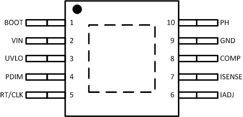
6 Pin Configuration and Functions
DGQ (HVSSOP) Package
Top View

Pin Functions
| PIN | TYPE(1) | DESCRIPTION | |
|---|---|---|---|
| NAME | NO. | ||
| BOOT | 1 | O | A bootstrap capacitor is required between BOOT and PH. If the voltage on this capacitor is below the minimum required by the output device, the output is forced to switch off until the capacitor is recharged. |
| COMP | 8 | O | Error amplifier output, and input to the output switch current comparator. Connect frequency compensation components to this pin. |
| GND | 9 | G | Ground. |
| IADJ | 6 | I | Analog current adjust pin. The voltage applied to this pin will set the current sense (ISENSE pin) voltage. The range of the ADJ pin is 180 mV to 1.8 V and the corresponding ISENSE pin voltage is the IADJ pin voltage divided by 6. |
| ISENSE | 7 | I | Inverting node of the transconductance (gM) error amplifier. |
| PDIM | 4 | I | PWM dimming input pin. The duty cycle of the PWM signal linearly controls the average output current of the converter. |
| PH | 10 | O | The source of the internal high-side MOSFET. |
| PowerPAD | PAD | G | GND pin must be electrically connected to the exposed pad directly beneath the device on the printed circuit board for proper operation. |
| RT/CLK | 5 | I | Resistor timing and external clock. An internal amplifier holds this pin at a fixed voltage when using an external resistor to ground to program the switching frequency. If the pin is pulled above the PLL upper threshold, a mode change occurs and the pin becomes a synchronization input. The internal amplifier is disabled and the pin becomes a high impedance clock input to the internal PLL. If the clocking edges stop, the internal amplifier is re-enabled and the mode returns to the resistor-programmed function. |
| UVLO | 3 | I | Adjustable undervoltage lockout. Set with resistor divider from VIN. |
| VIN | 2 | P | Input supply voltage, 4.5V to 42V or 4.5V to 60V for the HV version. |
(1) I = Input, O = Output, P = Supply, G = Ground