ZHCSDR0 April 2015 TPS92513 , TPS92513HV
PRODUCTION DATA.
- 1 特性
- 2 应用范围
- 3 说明
- 4 简化电路原理图
- 5 修订历史记录
- 6 Pin Configuration and Functions
- 7 Specifications
-
8 Detailed Description
- 8.1 Overview
- 8.2 Functional Block Diagram
- 8.3
Feature Description
- 8.3.1 Undervoltage Lockout and Low Power Shutdown (UVLO Pin)
- 8.3.2 Adjustable Switching Frequency (RT/CLK Pin)
- 8.3.3 Synchronizing the Switching Frequency to an External Clock (RT/CLK Pin)
- 8.3.4 Adjustable LED Current (IADJ and ISENSE Pins)
- 8.3.5 PWM Dimming (PDIM Pin)
- 8.3.6 External Compensation (COMP Pin)
- 8.3.7 Overcurrent Protection
- 8.3.8 Overtemperature Protection
- 8.4 Device Functional Modes
-
9 Application and Implementation
- 9.1 Application Information
- 9.2 Typical Application
- 9.3 Design Requirements
- 9.4
Detailed Design Procedure
- 9.4.1 Standard Component Selection
- 9.4.2 Calculate UVLO Resistor Values
- 9.4.3 Calculate the RT Resistor Value (RRT)
- 9.4.4 Calculate the ISENSE Resistor Value (R(ISENSE))
- 9.4.5 Calculate the Inductor Value and Operating Parameters (L)
- 9.4.6 Calculate the Minimum Input Capacitance and the Required RMS Current Rating (CIN)
- 9.4.7 Calculate the Output Capacitor Value (COUT)
- 9.4.8 Calculate the Diode Power Dissipation (D)
- 9.5 Application Curves
- 10Power Supply Recommendations
- 11Layout
- 12器件和文档支持
- 13机械、封装和可订购信息
8 Detailed Description
8.1 Overview
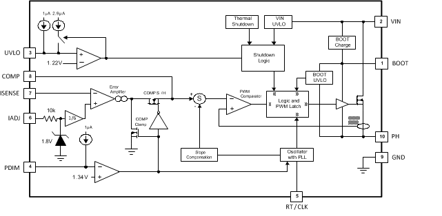
The TPS92513 is a high voltage, up to 1.5-A, step-down (buck) regulator with an integrated high-side N-channel MOSFET. To improve performance during line and load transients the device implements a constant frequency, peak-current mode control which reduces output capacitance and simplifies external frequency compensation design. The wide switching frequency of 100 kHz to 2000 kHz allows for efficiency and size optimization when selecting the output filter components.
8.2 Functional Block Diagram

8.3 Feature Description
8.3.1 Undervoltage Lockout and Low Power Shutdown (UVLO Pin)
The TPS92513 contains an internal under-voltage lockout circuit on the VIN pin of the device. However, this internal UVLO is for device protection only and does not contain hysteresis. The UVLO pin of the device should always be used to set the minimum VIN voltage that the circuit operates at. This level should be set using the minimum input voltage expected for the application with a minimum setting of 4.5 V.
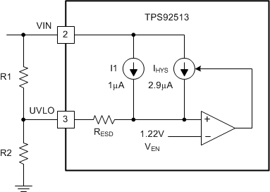
The UVLO pin has an internal pull-up current source of 1 µA (I1) that will provide a default ON state in the event the UVLO pin is left floating (not recommended). When the UVLO pin voltage exceeds 1.22 V (VEN), an additional 2.9 µA of hysteresis current is added (see Figure 11). This additional current provides the input voltage hysteresis. Use Equation 1 to set the external hysteresis (VHYS) for the input voltage. Use Equation 2 to set the input rising start voltage, VSTART. When the UVLO pin is pulled low, the internal regulators are shut down, the device enters a low-power shutdown mode and the compensation capacitor on the COMP pin, CCOMP, is discharged.
 Figure 11. Adjustable Undervoltage Lockout (UVLO)


8.3.2 Adjustable Switching Frequency (RT/CLK Pin)
The switching frequency of the TPS92513 is adjustable over a wide range from 100 kHz to 2 MHz by placing a resistor, RRT, on the RT/CLK pin. The RT/CLK pin voltage is typically 0.5 V and must have a resistor to ground to set the switching frequency. To determine the timing resistance for a given switching frequency, use Equation 5 or the curves in Figure 3 or Figure 4. To reduce the solution size one typically sets the switching frequency as high as possible, but tradeoffs of the supply efficiency, maximum input voltage and minimum controllable on time should be considered. The minimum controllable on time, tON(min), limits the maximum operating input voltage.


8.3.3 Synchronizing the Switching Frequency to an External Clock (RT/CLK Pin)
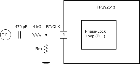
The RT/CLK pin can be used to synchronize the regulator to an external system clock by connecting a square wave to the RT/CLK pin through the circuit network as shown in Figure 12. The square wave amplitude must transition lower than 0.63 V and higher than 1.81 V on the RT/CLK pin and have an on-time greater than 51 ns and an off-time greater than 100 ns. The synchronization frequency range is 300 kHz to 2 MHz. The rising edge of the PH is synchronized to the falling edge of RT/CLK pin signal. The internal oscillator provides default switching frequency set by connecting the resistor from the RT/CLK pin to ground should the synchronization signal turn off.
It is required to AC couple the synchronization signal through a 470 pF ceramic capacitor and a 4 kΩ series resistor to the RT/CLK pin. The series resistor reduces PH jitter in heavy load applications when synchronizing to an external clock and in applications which transition from synchronizing to RT mode. The first time the RT/CLK pin is pulled above the CLK threshold the device switches from the RT resistor frequency to PLL mode. The internal 0.5 V voltage source is removed and the CLK pin becomes high impedance as the PLL starts to lock onto the external signal. Since there is a PLL on the regulator, the switching frequency can be higher or lower than the frequency set with the external resistor. The device transitions from the resistor mode to the PLL mode and then increases or decreases the switching frequency until the PLL locks onto the CLK frequency within 100 microseconds.
When the device transitions from the PLL to resistor mode, the switching frequency slows down from the CLK frequency to 150 kHz, then reapplies the 0.5 V voltage and the resistor then sets the switching frequency. It is not recommended that a system transition from PLL mode to resistor mode repeatedly during operation. When the PLL loses the external clock input the default 150 kHz switching frequency creates long on-times, which result in higher inductor ripple currents. This can lead to inductor saturation if the system is not designed to operate at this frequency.
 Figure 12. Frequency Synchronization
8.3.4 Adjustable LED Current (IADJ and ISENSE Pins)
The LED current can be set, and controlled dynamically, by using the IADJ pin of the TPS92513. Equation 7 shows the relationship between the voltage applied to IADJ (VIADJ) and the regulation setpoint at the ISENSE pin. Equation 8 shows how to calculate the value of the current setting resistor (RISENSE) from the ISENSE pin to ground for the desired LED current.


The IADJ pin voltage range is 0 V to 1.8 V and is internally clamped at 1.8 V. If analog current adjustment will not be used, the IADJ pin can be connected to VIN through a resistor for a default ISENSE voltage of 300 mV. This resistor should be sized so that the current into the IADJ pin is limited to 100 µA or less at the maximum input voltage. A precision reference between 0 V and 1.8 V can also be used on IADJ to control the ISENSE voltage. If no external voltage source is available, the IADJ pin can be tied to the RT/CLK pin either directly or using a resistor divider to generate a voltage between 0 V and 500 mV. If a resistor divider is used off the RT/CLK pin to generate the IADJ voltage it will introduce a parallel resistance with the RT resistor. High value resistors are recommended in that case and the parallel combination must be used to calculate the switching frequency. The current sense voltage is most accurate with IADJ voltages between 180 mV and 1.8 V for a dimming range of 10:1. Below 180 mV the TPS92513 dims well but may have more variation between circuits. Due to internal offsets pulling IADJ to 0 V will not result in a current sense voltage of 0 V. Some small current will continue to run unless the PDIM pin is pulled low or the device is disabled using the UVLO pin. Analog dimming is also most accurate when the device is in continuous conduction mode (CCM). If the highest accuracy possible is desired during analog dimming, size the inductor so that 1/2 the peak-to-peak inductor ripple is less than the minimum LED current to remain in CCM. The IADJ pin should be decoupled with a 10 nF capacitor to ground. A 1 kΩ resistor should be used between the ISENSE pin and RISENSE to protect the pin in the event RISENSE opens or there is a transient due to one or more LEDs shorting.
8.3.5 PWM Dimming (PDIM Pin)
The TPS92513 incorporates a PWM dimming input pin, which directly controls the enable/disable state of the internal gate driver. When PDIM is low, the gate driver is disabled. The PDIM pin has a 1 µA pull-up current source, which creates a default ON state when the PDIM pin is floating. When PDIM goes low, the gate driver shuts off and the LED current quickly reduces to zero. A square wave of variable duty cycle should be used and should have a low level below 0.79 V and a high level of 1.45 V or above.
The TPS92513 uses a sample-and-hold switch on the error amplifier output. During the PDIM off-time the COMP voltage remains unchanged. Also, the error amplifier output is internally clamped low. These techniques help the system recover to its regulation duty cycle quickly. The dimming frequency range is 100 Hz to 1 kHz and the minimum duty cycle is only limited in cases where the BOOT capacitor can discharge below its under-voltage threshold of 2 V (VIN is within 2 V of the total output voltage).
8.3.6 External Compensation (COMP Pin)
The TPS92513 error amplifier output is connected to the COMP pin. The TPS92513 is a simple device to stabilize and only requires a capacitor from the COMP pin to ground (CCOMP). A 0.1 µF capacitor is recommended and will work well for most all applications. If an application requires faster response to input voltage transients, a capacitor as small as 0.01 µF will work for most applications if needed. The overall system bandwidth can be approximated using Equation 9.

8.3.7 Overcurrent Protection
Overcurrent can be the result of a shorted sense resistor or a direct short from VOUT to GND. In either case, the voltage at the ISENSE pin is zero and this causes the COMP pin voltage to rise. When VCOMP reaches approximately 2.2 V, it is internally clamped and functions as a MOSFET current limit. The TPS92513 limits the MOSFET current to 6 A (typical). If the shorted condition persists, the TPS92513 junction temperature increases. If it increases above 165°C, the thermal shutdown protection is activated.
8.3.8 Overtemperature Protection
The TPS92513 includes a thermal shutdown circuit to protect the device from over-temperature conditions. The device can overheat due to high ambient temperatures, high internal power dissipation, or both. In the event the die temperature reaches 165°C the device will shut down until the die temperature falls 20°C at which point it will turn back on.
8.4 Device Functional Modes
8.4.1 Start-Up
To reduce inrush current and to keep the regulator in control during all startup conditions the TPS92513 employs a startup mode that behaves differently than during normal operation (regulation mode). The UVLO conditions must be satisfied before the TPS92513 is allowed to switch. When the UVLO pin is held low the device enters a low-power shutdown mode, and some internal circuits are deactivated to conserve power. When UVLO returns high these circuits are enabled, which results in a delay of approximately 50 µs (typical) before switching starts. During start-up the TPS92513 operates in a minimum pulse width mode which is an open-loop control. At the start of each switching cycle the internal oscillator initiates a SET pulse. The high-side MOSFET turns on with a minimum pulse width of 140 ns (typical), independent of the COMP voltage. The device does not pulse skip. While operating in minimum pulse width mode, the LED bypass capacitor is being charged causing an in-rush current. Also, the COMP voltage begins to rise as the error amplifier output current charges the compensation capacitor. When the COMP voltage reaches approximately 0.7 V, the error amplifier is ensured to be out of saturation and to have sufficient gain to regulate the loop. The TPS92513 then transitions from minimum pulse width mode to regulation mode. During regulation mode the error amplifier is now in closed-loop control of the system. The gain of the error amplifier quickly increases the duty cycle, which causes the output voltage to increase. Once the output voltage approaches the forward voltage of the LED string, the LED current quickly begins to increase until it reaches regulation.
There is a slight delay from the time the VIN and EN UVLO conditions are satisfied until the time the error amplifier has control of the feedback loop. This delay is a result of the time it takes COMP to charge the compensation capacitor to 0.7 V. This delay can be approximated as shown in Equation 10.

The peak inrush current, IPEAK, can be calculated to a first order approximation using Equation 11 and the value of the output capacitor, COUT.

8.4.2 Minimum Pulse Width and Limitations
The TPS92513 is designed to output a minimum pulse width during each switching cycle of 140 ns (typical). The control loop cannot regulate the system to an on-time less than this amount, and it does not skip pulses. When attempting to operate below the minimum on-time the system loses regulation and the LED current increases. This puts a practical limitation on the system operating conditions, as shown in Equation 12.

Where VOUT equals the forward voltage of the LED string plus the reference voltage VISENSE.
The system can avoid this operating condition by limiting the maximum input voltage as shown in Equation 12. If the input voltage cannot be limited due to application, then the switching frequency can be lowered, or the output voltage increased. This region of operation typically occurs with high input voltages, high operating frequencies, and low output voltages.
8.4.3 Maximum Duty Cycle and Bootstrap Voltage (BOOT)
The TPS92513 requires a small 0.1 µF ceramic capacitor between the BOOT and PH pins to provide the gate drive voltage for the high-side MOSFET. The BOOT capacitor is refreshed when the high-side MOSFET turns off, and the freewheeling rectifier diode conducts. A ceramic capacitor with an X7R or X5R dielectric and a minimum voltage rating of 10 V is recommended.
The TPS92513 is designed to operate up to 100% duty cycle as long as the BOOT to PH voltage is greater than at least 2 V. If the BOOT capacitor voltage drops below 2 V, then the BOOT UVLO circuit turns off the MOSFET, which allows the BOOT capacitor to be recharged. The current required from the BOOT capacitor to keep the MOSFET on is quite low. Therefore, many switching cycles occur before the BOOT capacitor is refreshed. In this way, the effective duty cycle of the converter is quite high.
Attention must be taken in maximum duty cycle applications which experience extended time periods with little or no load current such as during PWM dimming. When the voltage across the BOOT capacitor falls below the 2 V UVLO threshold, the high-side MOSFET is turned off, but there may not be enough inductor current to pull the PH pin down to recharge the BOOT capacitor. The high-side MOSFET of the regulator stops switching because the voltage across the BOOT capacitor is less than 2 V. The output capacitor then decays until the difference between the input voltage and output voltage is greater than 2 V, at which point the BOOT UVLO threshold is exceeded, and the device starts switching again until the desired output current is reached. This operating condition persists until the input voltage and/or the load current increases. It is recommended to adjust the VIN stop voltage, VSTOP, to be greater than the BOOT UVLO trigger condition at the minimum load of the application using the adjustable UVLO feature.
8.4.4 Thermal Shutdown and Thermal Limitations
The TPS92513 is a high current density device in a small package. Therefore; it is not capable of providing the full 1.5 A of output current under all conditions without the die reaching the thermal shutdown temperature. To ensure the device will not get too hot the package power dissipation should be calculated and used in conjunction with the device Thermal Information to estimate the maximum die temperature for a given application. The total device power dissipation can be closely approximated using the following equations:


Where each are in Watts and
- D is the maximum duty cycle (at minimum input voltage)
- VOUT is the LED stack voltage plus the reference voltage VISENSE
- PD(SW) is the power dissipated in the MOSFET
- PD(IQ) is the power dissipated by the internal circuitry
- PD(AC) are the approximate AC losses due to the MOSFET transitions
- PTOT is the total device dissipation