ZHCSFD3A April 2016 – August 2016 TPS92515 , TPS92515-Q1 , TPS92515HV , TPS92515HV-Q1
PRODUCTION DATA.
- 1 特性
- 2 应用
- 3 说明
- 4 修订历史记录
- 5 Device Comparison Table
- 6 Pin Configuration and Functions
- 7 Specifications
-
8 Detailed Description
- 8.1 Overview
- 8.2 Functional Block Diagram
- 8.3
Feature Description
- 8.3.1 General Operation
- 8.3.2 Current Sense Comparator
- 8.3.3 OFF Timer
- 8.3.4 OFF-Timer, Shunt FET Dimming or Shunted Output Condition
- 8.3.5 Internal N-channel MOSFET
- 8.3.6 VCC Internal Regulator and Undervoltage Lockout (UVLO)
- 8.3.7 Analog Adjust Input
- 8.3.8 Thermal Protection
- 8.3.9 Junction Temperature Relative Estimation
- 8.3.10 BOOT and BOOT UVLO
- 8.3.11 PWM (UVLO and Enable)
- 8.4 Device Functional Modes
-
9 Application and Implementation
- 9.1 Application Information
- 9.2
Typical Application
- 9.2.1 General Design Procedure
- 9.2.2 Design Requirements
- 9.2.3
Detailed Design Procedure
- 9.2.3.1 Calculating Duty Cycle
- 9.2.3.2 Calculate OFF-Time Estimate
- 9.2.3.3 Calculate OFF-Time Resistor ROFF
- 9.2.3.4 Calculate the Inductance Value
- 9.2.3.5 Calculate the Sense Resistance
- 9.2.3.6 Calculate Input Capacitance
- 9.2.3.7 Verify Peak Current for Inductor Selection
- 9.2.3.8 Calculate Output Capacitance
- 9.2.3.9 Calculate UVLO Resistance Values
- 9.2.4 Application Curves
- 9.3 Dos and Don'ts
- 10Power Supply Recommendations
- 11Layout
- 12器件和文档支持
- 13机械、封装和可订购信息
11 Layout
11.1 Layout Guidelines
The performance of any switching converter depends as much upon the layout of the PCB as the component selection. Following a few simple guidelines maximizes noise rejection and minimizes the generation of EMI within the circuit.
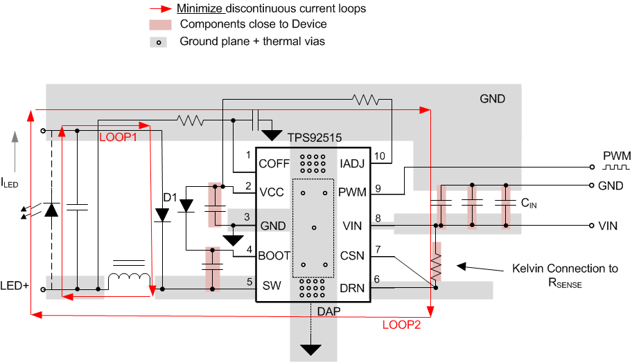
Figure 44 shows a sample layout and the associated current loops.
- Discontinuous currents are the type of current most likely to generate EMI, therefore care should be taken when routing these paths.
- The main path for discontinuous current contains the input capacitor (CIN), the recirculating diode (D1), the internal MOSFET (DRN pin to SW pin), and the sense resistor (RSENSE) shown as LOOP2. Make LOOP2 as small as possible.
- Make the connections between all three components short and thick to minimize parasitic inductance. In particular, the switch node (where L1, D1 and the SW pin connect, shown as LOOP1) should be only large enough to connect the components without excessive heating from the current it carries.
- The IADJ, COFF, CSN and VIN pins are all high-impedance control inputs, therefore minimize the loops containing these high impedance nodes. The most sensitive loop contains the sense resistor (RSENSE) Place the sense resistor as close as possible to the CSN and VIN pins to maximize noise rejection.
- Place the OFF-time capacitor (connected from the COFF pin to ground) close to the COFF and GND pins to maximize noise rejection.
- If external resistors are used to bias the IADJ pin, they should also be placed close to the IADJ and GND pins and could be decoupled with a small capacitor.
- In some applications the LED load can be far away (several inches or more) from the device, or on a separate PCB connected by a wiring harness. When an output capacitor is used and the LED load is large or separated from the main converter, the output capacitor should be placed close to the LEDs to reduce the effects of parasitic inductance on the AC impedance of the capacitor.
11.2 Layout Example
 Figure 44. TPS92515 Layout Example