ZHCSIY0 October 2018 TPS92515AHV-Q1
PRODUCTION DATA.
- 1 特性
- 2 应用
- 3 说明
- 4 修订历史记录
- 5 Device Comparison Table
- 6 Pin Configuration and Functions
- 7 Specifications
-
8 Detailed Description
- 8.1 Overview
- 8.2 Functional Block Diagram
- 8.3
Feature Description
- 8.3.1 General Operation
- 8.3.2 Current Sense Comparator
- 8.3.3 OFF Timer
- 8.3.4 OFF-Timer, Shunt FET Dimming or Shunted Output Condition
- 8.3.5 Internal N-channel MOSFET
- 8.3.6 VCC Internal Regulator and Undervoltage Lockout (UVLO)
- 8.3.7 Analog Adjust Input
- 8.3.8 Thermal Protection
- 8.3.9 Junction Temperature Relative Estimation
- 8.3.10 BOOT and BOOT UVLO
- 8.3.11 PWM (UVLO and Enable)
- 8.4 Device Functional Modes
-
9 Application and Implementation
- 9.1 Application Information
- 9.2
Typical Application
- 9.2.1 General Design Procedure
- 9.2.2 Design Requirements
- 9.2.3
Detailed Design Procedure
- 9.2.3.1 Calculating Duty Cycle
- 9.2.3.2 Calculate OFF-Time Estimate
- 9.2.3.3 Calculate OFF-Time Resistor ROFF
- 9.2.3.4 Calculate the Inductance Value
- 9.2.3.5 Calculate the Sense Resistance
- 9.2.3.6 Calculate Input Capacitance
- 9.2.3.7 Verify Peak Current for Inductor Selection
- 9.2.3.8 Calculate Output Capacitance
- 9.2.3.9 Calculate UVLO Resistance Values
- 9.2.4 Application Curves
- 9.3 Dos and Don'ts
- 10Power Supply Recommendations
- 11Layout
- 12器件和文档支持
- 13机械、封装和可订购信息
8.3.1 General Operation
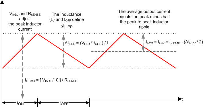
The TPS92515AHV-Q1 operates using a peak-current, constant OFF-time as described in Figure 11. Two states dictate the high-side FET control. The switch remains on until the programmed peak current is reached. The device controls the peak current by monitoring the voltage across the sense resistor. When the voltage drop is higher than the programmed threshold, the peak current is reached, and the switch is turned OFF, which begins the OFF-time period. A capacitor on the COFF pin is then charged through a resistor connected to the output. When the COFF pin voltage reaches the 1-V (typical) threshold, the OFF-time ends. The COFF pin capacitor resets and the main switch turns ON, and the next cycle begins.
 Figure 11. Hysteretic Operation
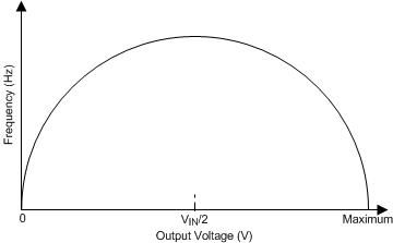
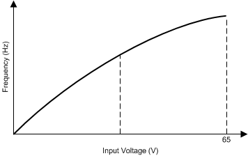
 Although commonly referred to as constant OFF-time, it is the output votage that determines the OFF-time. This connection ensures constant peak-to-peak ripple. To maintain a constant ripple over various input and output voltages, the converter OFF-time becomes shorter or longer resulting in a change in frequency. If the input voltage and output voltage are relatively constant, the frequency also remains constant. If either the input voltage or the output voltage changes, the frequency changes. For a fixed input voltage, the device operates at the maximum frequency at 50% duty cycle and the frequency reduces as the duty cycle becomes shorter or longer. A graphical representation is shown in Figure 12. For a fixed output voltage (VLED), the frequency is always the maximum at the highest input voltage as shown in Figure 13.

| Fixed input voltage |

| Fixed LED voltage |
Because the OFF-time is proportional to the output voltage, it is possible to illustrate how VLED can be removed from the output current equation. When VLED >> VOFT , the output ripple can be defined as shown in Equation 1.
where
- dt is defined by the OFF-timer
.

Substitute dt in Equation 1 to create Equation 3.


When VLED >≈ 10 V, use the ILED calculation Equation 4. The Detailed Design Procedure section describes a design example that uses the more detailed equation. A VLED > 10 V ensures a linear charging ramp below 1 V. If VLED <≈10 V, use Equation 5 that considers the exponential charging characteristic.

Because the control method relies on thresholds to control the main switch, offsets and delays must also be considered when examining the output accuracy. The ILED equation can be expanded to include these error sources as shown in Equation 6. ILED equations include several passive components, so it is important to consider the tolerance of each component. The VCST_Offset parameter is the variation in the VCST threshold between the typical and maximum or minimum values as defined in the Electrical Characteristics table.
