ZHCSIY0 October 2018 TPS92515AHV-Q1
PRODUCTION DATA.
- 1 特性
- 2 应用
- 3 说明
- 4 修订历史记录
- 5 Device Comparison Table
- 6 Pin Configuration and Functions
- 7 Specifications
-
8 Detailed Description
- 8.1 Overview
- 8.2 Functional Block Diagram
- 8.3
Feature Description
- 8.3.1 General Operation
- 8.3.2 Current Sense Comparator
- 8.3.3 OFF Timer
- 8.3.4 OFF-Timer, Shunt FET Dimming or Shunted Output Condition
- 8.3.5 Internal N-channel MOSFET
- 8.3.6 VCC Internal Regulator and Undervoltage Lockout (UVLO)
- 8.3.7 Analog Adjust Input
- 8.3.8 Thermal Protection
- 8.3.9 Junction Temperature Relative Estimation
- 8.3.10 BOOT and BOOT UVLO
- 8.3.11 PWM (UVLO and Enable)
- 8.4 Device Functional Modes
-
9 Application and Implementation
- 9.1 Application Information
- 9.2
Typical Application
- 9.2.1 General Design Procedure
- 9.2.2 Design Requirements
- 9.2.3
Detailed Design Procedure
- 9.2.3.1 Calculating Duty Cycle
- 9.2.3.2 Calculate OFF-Time Estimate
- 9.2.3.3 Calculate OFF-Time Resistor ROFF
- 9.2.3.4 Calculate the Inductance Value
- 9.2.3.5 Calculate the Sense Resistance
- 9.2.3.6 Calculate Input Capacitance
- 9.2.3.7 Verify Peak Current for Inductor Selection
- 9.2.3.8 Calculate Output Capacitance
- 9.2.3.9 Calculate UVLO Resistance Values
- 9.2.4 Application Curves
- 9.3 Dos and Don'ts
- 10Power Supply Recommendations
- 11Layout
- 12器件和文档支持
- 13机械、封装和可订购信息
8.3.4 OFF-Timer, Shunt FET Dimming or Shunted Output Condition
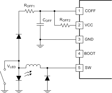
The OFF-time is derived from the output voltage to create a constant inductor ripple. A constant inductor ripple ensures linearity when dimming. When the dimming method selected requires the output to be shorted, (shunt FET or Switched Matrix approach) it is necessary to derive the OFF-time ramp from an alternate source. When the output is shunted, the output voltage becomes very low and possibly less than the 1 V OFF-timer threshold voltage. If this occurs, the off timer is not able to trip and the OFF-time reaches the maximum OFF-time before the switch is turned on again. The system is able to operate in this mode, but constant inductor current ripple and linear shunt-FET dimming is not possible. To avoid this situation, VCC can be used as a parallel source to charge the COFF capacitor and maintain a constant ripple even when the output is shorted. This ensures precise dimming linearity. Refer to Figure 14 for connection information.
It is not recommended to apply power to the OFF-timer circuitry while the VIN pin is not powered. The device includes an internal diode between the COFF pin and the VCC pin. If the COFF pin receives power with no input voltage (VIN) applied, VCC pin voltage could inadvertently be pulled up and cause the device to attempt operation. This attempt could negatively affect the application if this operation is not desired.
Selecting the value for ROFF2 is a two-step process.
The first step is to compute the OFF-time required when the output is shunted (tOFF-Shunt).

where
- VSHUNT is the output voltage when the shunt device or LED Matrix device is ON
The second steps is to compute ROFF2 using (tOFF-Shunt).

The value of ROFF1 becomes the previously calculated value of ROFF.
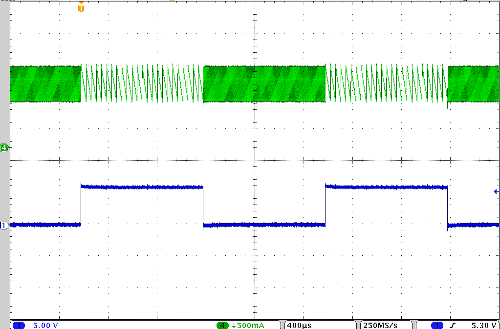
The result of these calculations produce an inductor current that maintains the same DC value when shunted or when not shunted as shown in Figure 15.
 Figure 14. Shunt Dimming COFF Connection
| Ch1: PWM Signal | Time: 400 µs/div |
| Ch4: Inductor current | No Output Capacitor |