ZHCSIY0 October   2018 TPS92515AHV-Q1

PRODUCTION DATA.  

  1. 特性
  2. 应用
  3. 说明
    1.     简化的降压 LED 驱动器应用
  4. 修订历史记录
  5. Device Comparison Table
  6. Pin Configuration and Functions
    1.     Pin Functions
  7. Specifications
    1. 7.1 Absolute Maximum Ratings
    2. 7.2 ESD Ratings
    3. 7.3 Recommended Operating Conditions
    4. 7.4 Thermal Information
    5. 7.5 Electrical Characteristics
    6. 7.6 Typical Characteristics
  8. Detailed Description
    1. 8.1 Overview
    2. 8.2 Functional Block Diagram
    3. 8.3 Feature Description
      1. 8.3.1  General Operation
      2. 8.3.2  Current Sense Comparator
      3. 8.3.3  OFF Timer
      4. 8.3.4  OFF-Timer, Shunt FET Dimming or Shunted Output Condition
      5. 8.3.5  Internal N-channel MOSFET
        1. 8.3.5.1 Drop-Out
      6. 8.3.6  VCC Internal Regulator and Undervoltage Lockout (UVLO)
      7. 8.3.7  Analog Adjust Input
        1. 8.3.7.1 IADJ Pin Clamp
        2. 8.3.7.2 IADJ Pin Clamp Characteristic
        3. 8.3.7.3 Analog Adjust (IADJ Pin) Control Methods
        4. 8.3.7.4 IADJ Control Method Notes
      8. 8.3.8  Thermal Protection
        1. 8.3.8.1 Maximum Output Current and Junction Temperature
      9. 8.3.9  Junction Temperature Relative Estimation
      10. 8.3.10 BOOT and BOOT UVLO
        1. 8.3.10.1 Start-Up, BOOT-UVLO and Pre-Charged Condition
      11. 8.3.11 PWM (UVLO and Enable)
        1. 8.3.11.1 Using PWM for UVLO (Undervoltage Lockout) Protection
          1. 8.3.11.1.1 UVLO Programming Resistors
        2. 8.3.11.2 Using PWM for Digitally Controlled Enable
        3. 8.3.11.3 UVLO: VIN, VCC and BOOT UVLO
        4. 8.3.11.4 Analog and PWM Dimming - Normalized Results and Comparison
    4. 8.4 Device Functional Modes
  9. Application and Implementation
    1. 9.1 Application Information
    2. 9.2 Typical Application
      1. 9.2.1 General Design Procedure
        1. 9.2.1.1 Calculating Duty Cycle
        2. 9.2.1.2 Calculate OFF-Time Estimate
        3. 9.2.1.3 Calculate OFF-Time Resistor ROFF
        4. 9.2.1.4 Calculate the Minimum Inductance Value
        5. 9.2.1.5 Calculate the Sense Resistance
        6. 9.2.1.6 Calculate Input Capacitance
        7. 9.2.1.7 Calculate Output Capacitance
      2. 9.2.2 Design Requirements
      3. 9.2.3 Detailed Design Procedure
        1. 9.2.3.1 Calculating Duty Cycle
        2. 9.2.3.2 Calculate OFF-Time Estimate
        3. 9.2.3.3 Calculate OFF-Time Resistor ROFF
        4. 9.2.3.4 Calculate the Inductance Value
        5. 9.2.3.5 Calculate the Sense Resistance
        6. 9.2.3.6 Calculate Input Capacitance
        7. 9.2.3.7 Verify Peak Current for Inductor Selection
        8. 9.2.3.8 Calculate Output Capacitance
        9. 9.2.3.9 Calculate UVLO Resistance Values
      4. 9.2.4 Application Curves
    3. 9.3 Dos and Don'ts
  10. 10Power Supply Recommendations
    1. 10.1 Input Source Direct from Battery
    2. 10.2 Input Source from a Boost Stage
  11. 11Layout
    1. 11.1 Layout Guidelines
    2. 11.2 Layout Example
  12. 12器件和文档支持
    1. 12.1 文档支持
      1. 12.1.1 相关文档
        1. 12.1.1.1 相关链接
    2. 12.2 接收文档更新通知
    3. 12.3 社区资源
    4. 12.4 商标
    5. 12.5 静电放电警告
    6. 12.6 术语表
  13. 13机械、封装和可订购信息

封装选项

机械数据 (封装 | 引脚)
散热焊盘机械数据 (封装 | 引脚)
订购信息

Calculate UVLO Resistance Values

Consider the rising threshold of VIN to be 29 V and the hysteresis to be 4 V, calculate R2 and R3 to create the desired operation:

Equation 33. TPS92515AHV-Q1 R3_UVLO_numbers.gif
Equation 34. TPS92515AHV-Q1 R2_UVLO_numbers.gif

The final schematic is shown in Figure 33 and performance curves in the Application Curves section:
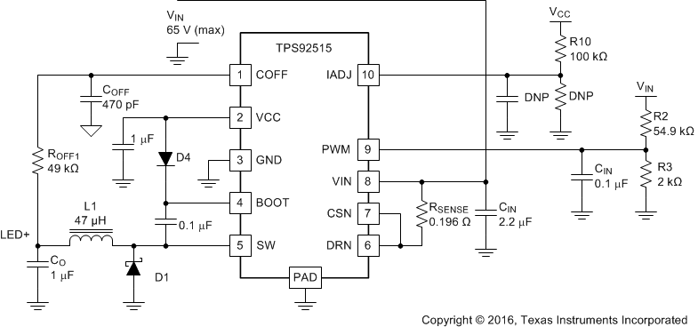
TPS92515AHV-Q1 TypAppSchematic_numbers.gifFigure 33. Application Schematic