ZHCSFD3A April 2016 – August 2016 TPS92515 , TPS92515-Q1 , TPS92515HV , TPS92515HV-Q1
PRODUCTION DATA.
- 1 特性
- 2 应用
- 3 说明
- 4 修订历史记录
- 5 Device Comparison Table
- 6 Pin Configuration and Functions
- 7 Specifications
-
8 Detailed Description
- 8.1 Overview
- 8.2 Functional Block Diagram
- 8.3
Feature Description
- 8.3.1 General Operation
- 8.3.2 Current Sense Comparator
- 8.3.3 OFF Timer
- 8.3.4 OFF-Timer, Shunt FET Dimming or Shunted Output Condition
- 8.3.5 Internal N-channel MOSFET
- 8.3.6 VCC Internal Regulator and Undervoltage Lockout (UVLO)
- 8.3.7 Analog Adjust Input
- 8.3.8 Thermal Protection
- 8.3.9 Junction Temperature Relative Estimation
- 8.3.10 BOOT and BOOT UVLO
- 8.3.11 PWM (UVLO and Enable)
- 8.4 Device Functional Modes
-
9 Application and Implementation
- 9.1 Application Information
- 9.2
Typical Application
- 9.2.1 General Design Procedure
- 9.2.2 Design Requirements
- 9.2.3
Detailed Design Procedure
- 9.2.3.1 Calculating Duty Cycle
- 9.2.3.2 Calculate OFF-Time Estimate
- 9.2.3.3 Calculate OFF-Time Resistor ROFF
- 9.2.3.4 Calculate the Inductance Value
- 9.2.3.5 Calculate the Sense Resistance
- 9.2.3.6 Calculate Input Capacitance
- 9.2.3.7 Verify Peak Current for Inductor Selection
- 9.2.3.8 Calculate Output Capacitance
- 9.2.3.9 Calculate UVLO Resistance Values
- 9.2.4 Application Curves
- 9.3 Dos and Don'ts
- 10Power Supply Recommendations
- 11Layout
- 12器件和文档支持
- 13机械、封装和可订购信息
8 Detailed Description
8.1 Overview
The TPS92515 is an internal N-channel MOSFET (monolithic NFET) hysteric control, buck regulator. Hysteretic operation allows a high control bandwidth and is ideal for shunt FET and LED matrix applications (series LED switched network). The high-side differential current sense with low adjustable threshold voltage via a 10:1 divider, provides an excellent method for regulating output current while maintaining high system efficiency. The device uses a controlled OFF-time (COFT) architecture to allow the converter to operate in both continuous conduction mode (CCM) and discontinuous conduction mode (DCM) with no external control loop compensation, and provides an inherent cycle-by-cycle current limit.
The adjustable current sense threshold provides the capability for analog dimming the LED current over the full range and the PWM dimming input allows for high-frequency PWM dimming control requiring no external components. Configuration options allow for easy implementation of external shunt FET dimming. See also the OFF-Timer, Shunt FET Dimming or Shunted Output Condition section.
The device does not internally limit the maximum attainable average LED current. It does have a thermal limit based on the maximum junction temperature. The maximum junction temperature is a function of the system operating points (efficiency, ambient temperature, thermal management), component choices, and switching frequency. This functionality allows the device to provide constant currents up to 1 A in a wide variety of applications and up to 2 A in a smaller sub-set of applications. This simple regulator contains all the features necessary to implement a high-efficiency, versatile, high-performance LED driver.
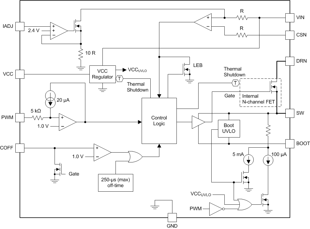
8.2 Functional Block Diagram
8.3 Feature Description
8.3.1 General Operation
The TPS92515 operates using a peak-current, constant OFF-time as described in Figure 11. Two states dictate the high-side FET control. The switch turns on and stays on until the programmed peak current is reached. The peak current is controlled by monitoring the voltage across the sense resistor. When the voltage drop is higher than the programmed threshold, the peak current is reached, and the switch is turned OFF, which initiates the OFF-time period. A capacitor on the COFF pin is then charged through a resistor connected to the output. When the COFF pin voltage reaches the 1-V (typical) threshold, the OFF-time ends. The COFF pin capacitor resets and the main switch turns ON, and the next cycle begins.
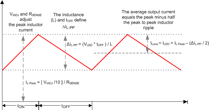 Figure 11. Hysteretic Operation
Although commonly referred to as constant OFF-time, the OFF-time control voltage is normally derived from the output voltage. This connection ensures constant peak-to-peak ripple. To maintain a constant ripple over various input and output voltages, the converter OFF-time becomes shorter or longer resulting in a change in frequency. If the input voltage and output voltage are relatively constant, the frequency also remains constant. If either the input voltage or the output voltage changes, the frequency changes. For a fixed input voltage, the device operates at the maximum frequency at 50% duty cycle and the frequency reduces as the duty cycle becomes shorter or longer. A graphical representation is shown in Figure 12. For a fixed output voltage (VLED), the frequency is always the maximum at the highest input voltage as shown in Figure 13.
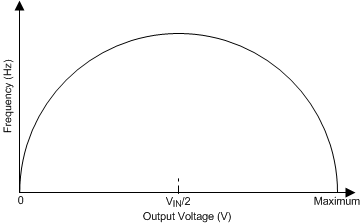
| Fixed input voltage |
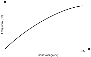
| Fixed LED voltage |
By making the OFF-time proportional to the output voltage, it is possible to illustrate how VLED can be removed from the output current equation. When VLED >> VOFT , the output ripple can be defined as shown in Equation 1.
where
- dt is defined by the OFF-timer
.

Substitute dt in Equation 1 to create Equation 3.


When VLED >≈ 10 V, use the ILED calculation Equation 4. The Detailed Design Procedure section describes a design example that uses the more detailed equation. A VLED > 10 V ensures a linear charging ramp below 1 V. If VLED <≈10 V, use Equation 5 that considers the exponential charging characteristic.

Because the control method relies on thresholds to control the main switch, offsets and delays must also be considered when examining the output accuracy. The ILED equation can be expanded to include these error sources as shown in Equation 6. ILED equations include several passive components, so it is important to consider the tolerance of each component. The VCST_Offset parameter is the variation in the VCST threshold between the typical and maximum or minimum values as defined in the Electrical Characteristics table.

8.3.2 Current Sense Comparator
A comparator, two resistors and a current source create a peak current detection circuit block. See the Functional Block Diagram for details. A current source controlled by VIADJ draws a current across a resistor in series with a comparator, forcing a proportional offset. The resistor in the current source (10 R) and in series with the comparator (R) are sized with a 10:1 ratio. This ratio allows for a practical voltage range of operation for the IADJ pin and maintains a small current sense voltage for low losses and less impact on efficiency.
The ON cycle begins with the offset in place via IADJ across the resistor R at the VIN pin. When the current rises enough to create a voltage across the sense resistor to match the offset, the comparator trips. The end of the ON-time period starts an OFF-time cycle.
Trace resistance can have an impact on accuracy, so care should be used when routing the traces to VIN and CSN from the sense resistor. Because the sense resistor value is typically in milli-ohms, use a short kelvin connection to CSN and place the sense resistor as close as possible to VIN.
8.3.3 OFF Timer
The converter OFF-time is controlled via the COFF pin. The output voltage charges a capacitor to 1 V through a resistor creating a delay. Deriving the OFF-time from the output voltage creates a ramp representing the inductor current. If the output voltage cannot be used, another voltage fixed source may be implemented to create a truly constant OFF-time. However, this configuration reduces output current accuracy. When the device is first enabled (when VCC rises above the VCC undervoltage lockout threshold) the pull-down on the COFF pin is disabled, allowing a voltage to build up on the COFF capacitor. At the same time, the maximum off timer begins. If the voltage source is sufficiently above the 1-V threshold, the ramp becomes linear and approximates the inductor current. If the 1-V nominal COFF threshold is reached, or the COFF capacitor charge time duration is greater than tOFF(max) (maximum OFF-time timer expires), a switching cycle starts.
The timer reaches the maximum OFF-time during start-up when the output is completely discharged or when shunt FET dimming and the shunt FET shunts the output for the required period.
Equation 7 calculates ROFF for a desired OFF-time.

8.3.4 OFF-Timer, Shunt FET Dimming or Shunted Output Condition
The OFF-time is derived from the output voltage to create a constant inductor ripple. A constant inductor ripple ensures linearity when dimming. When the dimming method selected requires the output to be shorted, (shunt FET or Switched Matrix approach) it is necessary to derive the OFF-time ramp from an alternate source. When the output is shunted, the output voltage becomes very low and possibly less than the 1 V OFF-timer threshold voltage. If this occurs, the off timer is not able to trip and the OFF-time reaches the maximum OFF-time before the switch is turned on again. The system is able to operate in this mode, but constant inductor current ripple and linear shunt-FET dimming is not possible. To avoid this situation, VCC can be used as a parallel source to charge the COFF capacitor and maintain a constant ripple even when the output is shorted. This ensures precise dimming linearity. Refer to Figure 14 for connection information.
It is not recommended to apply power to the OFF-timer circuitry while the VIN pin is not powered. The device includes an internal diode between the COFF pin and the VCC pin. If the COFF pin receives power with no input voltage (VIN) applied, VCC pin voltage could inadvertently be pulled up and cause the device to attempt operation. This attempt could negatively affect the application if this operation is not desired.
Selecting the value for ROFF2 is a two-step process.
The first step is to compute the OFF-time required when the output is shunted (tOFF-Shunt).

where
- VSHUNT is the output voltage when the shunt device or LED Matrix device is ON
The second steps is to compute ROFF2 using (tOFF-Shunt).

The value of ROFF1 becomes the previously calculated value of ROFF.
The result of these calculations produce an inductor current that maintains the same DC value when shunted or when not shunted as shown in Figure 15.
 Figure 14. Shunt Dimming COFF Connection
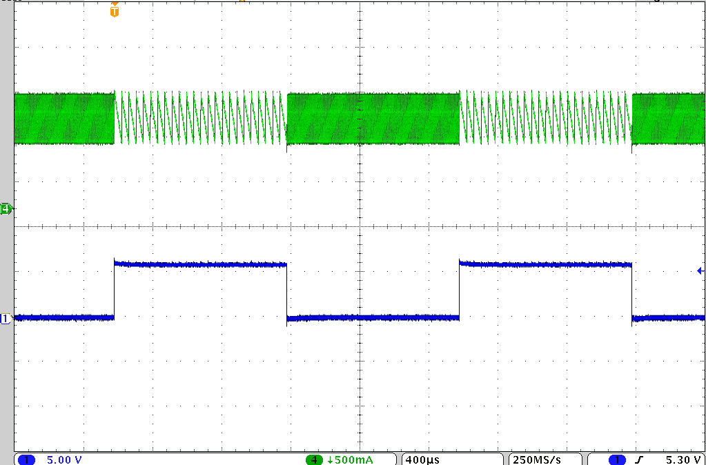
| Ch1: PWM Signal | Time: 400 µs/div |
| Ch4: Inductor current | No Output Capacitor |
8.3.5 Internal N-channel MOSFET
Integrated in the TPS92515 is a low on-resistance (RDS(on)) N-channel MOSFET. The resistance specified in the Electrical Characteristics table for the drive voltage and temperature is important to consider because the actual on-resistance for a given operating point affects efficiency and the transition point into drop-out when operating at high currents. A sensing element for thermal shutdown circuitry has been located close to the internal FET to better assist in part protection.
8.3.5.1 Drop-Out
The TPS92515 can operate safely even when the input voltage enters the drop-out region. As VIN approaches VLED, ΔIL-PP falls to a level much lower than during normal operation. Because the average output current is based on Equation 10, as ΔIL-PP becomes smaller, the average current tends to increase. The amount of increase depends on the value of ΔIL-PP used in the design. If drop-out performance is a concern, performance can be improved by lowering the ΔIL-PP design parameter.
8.3.6 VCC Internal Regulator and Undervoltage Lockout (UVLO)
The device incorporates a linear regulator to generate the 5-V (typ) VCC voltage. The VCC output voltage is monitored to implement undervoltage lockout (UVLO) protection. The UVLO thresholds are fixed and cannot be adjusted. The device has been designed to supply current for the device operation as well as additional power for external circuitry. If a 5-V rail is required in an application, the device can allow up to 500 µA to be drawn in addition to the device load. A capacitance of 1 µF or ≥ 10× the BOOT capacitance to a maximum of 10 µF is recommended.
The device requires adequate input decoupling in order to lower ΔVIN-PP ripple for the best VCC supply voltage performance. ΔVIN-PP must not exceed 10% of the input voltage VIN or 2 V, whichever is lower.
8.3.7 Analog Adjust Input
The analog adjust pin (IADJ) provides the reference for the peak current trip point. Through the use of an internal 10:1 divider, a wider range and finer control of the peak current sense threshold is created. For example, applying 2.2 V to the IADJ pin creates a 220-mV, peak-current-sense trip point. The lower sense voltage also lowers the power (V2/R) losses at the sense resistor. There is a practical lower limit to the IADJ pin voltage choice due to circuit non-idealities. For example, using VIADJ = 0.5 V results in a sense voltage of 50 mV, which does not allow accurate operation.
8.3.7.1 IADJ Pin Clamp
The IADJ pin incorporates an internal 2.4-V clamp. An area of inaccuracy in the clamp knee point voltage requires the designer to consider how to mitigate this situation when selecting an IADJ pin voltage. The most accurate method is to apply 2.2 V to the IADJ pin, which allows it to remain below the clamp knee-point voltage area. If an accurate, external, 2.2-V (or lower) reference is not available, use the next most accurate control method which is the internal clamp. The least accurate method uses a resistor divider on the VCC pin. The Analog and PWM Dimming - Normalized Results and Comparison section includes measured analog dimming results.
8.3.7.2 IADJ Pin Clamp Characteristic
Figure 16 shows the clamping characterization. Figure 28 shows an application measurement. The translation is straightforward, with the exception of the knee-point voltage area. For voltages ≤2.2 V, the internal VIN to CSN peak current sense voltage equals VIADJ/10. For voltages ≥ 2.4 V the voltage equals 240 mV. For the area 2.2 ≤ VIADJ≤ 2.4 the voltage approximates VIADJ/10, but varies slightly more than the other regions of operation.
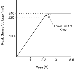 Figure 16. IADJ Pin Internal Clamp Characteristic
8.3.7.3 Analog Adjust (IADJ Pin) Control Methods
This section describes several analog adjust (IADJ) control methods configurations.
Table 1. IADJ Pin Connection Schematics
| FIGURE | IADJ PIN CONNECTION |
|---|---|
| Figure 17 | IADJ pin tied directly to the VCC pin using the internal 2.4-V clamp. |
| Figure 18 | IADJ pin tied through a voltage divider to the VCC pin allowing a lower peak current sense voltage |
| Figure 19 | IADJ pin tied through a resistor and thermistor divider, implementing thermal foldback function. |
| Figure 20 | IADJ pin is connected to a micro controller. A GPI/GPIO is connected to a filter to create an analog adjust voltage. |
| Figure 21 | IADJ pin connection to implement a soft-start sequence |
| Figure 22 | IADJ pin is connected to a precision reference. This configuration yields the highest accuracy. |
.
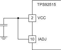 Figure 17.
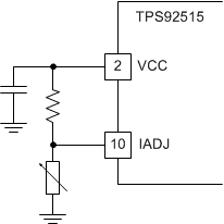 Figure 19.
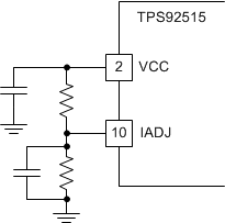 Figure 21.
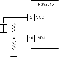 Figure 18.
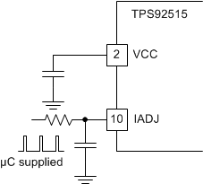 Figure 20.
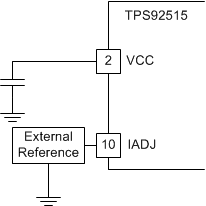 Figure 22.
8.3.7.4 IADJ Control Method Notes
- Connecting the IADJ pin directly to VCC is simple and is the most accurate stand-alone implementation.
- Using a resistor divider circuit can lower the sense voltage and improve efficiency if the converter output currents are high. The trade-off is an increased variation in the peak trip voltage. Note that there are also practical limitations to how low the sense voltage can be and maintain a reasonable accuracy.
- The simple thermal foldback method sizes the divider to set the IADJ voltage above 2.4 V. This method uses the internal clamp when thermal foldback is not required and sets the IADJ voltage below 2.4 V when foldback is required. Match the temperature characteristic of the thermistor to the second resistor in the divider. As an alternative, use a positive temperature coefficient (PTC) thermistor as the upper resistor in the divider.
- By using a micro-controller to control the timing output, the duty cycle can be controlled and the voltage can be filtered and connected to the IADJ pin. Use a filter pole of 1/10th the micro-controller control pin output switching frequency, or use R ≈ 1 kΩ and C ≈ 4.7 µF as a starting point.
- Simply add a capacitor to the IADJ pin and size the R-C constant to produce the desired soft-start time. Consider the maximum current is reached when VIADJ = 2.4 V.
- To achieve the highest accuracy, use an external, high-precision reference and power it from the TPS92515 VCC if required. A 1% or 2% Zener diode, TL431 device, or an existing precision reference circuit can be used.
8.3.8 Thermal Protection
The TPS92515 device incorporates thermal protection circuitry. If the TPS92515 thermal pad is not soldered, or not soldered correctly, the device reaches the thermal shutdown temperature prematurely. Use X-ray inspection or some other means to verify the device thermal pad soldering to ensure correct assembly.
Two internal sensing elements ensure proper temperature measurement across the die. One sensing element is located near the internal FET. The other sensing element is located near the VCC regulator. Power dissipation the FET and internal regulator contribute the most to device temperature rise.
When the device temperature reaches the thermal shut-down level at the FET sense point, the high-side FET and internal regulator become disabled and switching stops. When thermal shut-down temperature is reached at the regulator sense point, the VCC regulator becomes disabled, and switching stops when VCC falls below the VCCUVLO level. In both cases, after the device lowers 10°C (typical) from the trip temperature, normal operation resumes.
8.3.8.1 Maximum Output Current and Junction Temperature
As with all power converter controllers and regulators, practical limits to specification maximums must be considered for each application. For example, it is not possible to operate the TPS92515 with a switching frequency of 1 MHz, output current of 2 A, at an ambient temperature of 125°C and stay within operating limits. Conversion factors and environment must be considered. This section describes two conversion scenarios with different operating conditions that would result in approximately the same junction temperature. In each case all of the power loss factors combine to develop the device junction temperature.
Figure 24 describes a design with half the output current and a lower switching frequency compared to that shown in Figure 23. However, the design shown in Figure 24 has a higher ambient temperature, higher VIN and an additional external VCC load, resulting in similar junction temperature. Table 2 lists trade-offs and impact on temperature. In general, applications requiring high current (2 A) or a high switching frequency (> 1 MHz) provide reduced maximum ambient temperature levels.
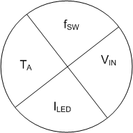
| ILED = 1 A | VIN = 14 V |
| fSW = 500 kHz | TA = 85°C |
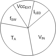
| ILED = 500 mA | TA = 125°C |
| fSW = 300 kHz | External VCC load = 500 µA |
| VIN = 60 V |
Table 2. Device Junction Temperature Factors
| FACTOR | AFFECT ON TEMPERATURE AND TRADE-OFFS | |
|---|---|---|
| TA | Ambient temperature | An increase in the ambient temperatre will increase the junction temperature by the same amount. |
| VIN | Input voltage | A higher input voltage results in more power developed across the internal regulator resulting in higher internal losses. A higher voltage often yields a larger step-down conversion and lower efficiency. |
| ILED | LED current | A higher LED output current results in higher power (I2R) losses in current carrying elements like the internal MOSFET. |
| IVCC(ext) | External VCC current | Current used to supply additional loads external to the TPS92515 device draw from the internal regulator. More external current results in an increased junction temperature. When an external source supplies the BOOT current internal power dissipation decreases. |
| fSW | Switching frequency | Each time the internal FET is turned ON and OFF, current must flow from VCC to the gate driver. The current drawn by a switching gate approximately equals the gate charge times the switching frequency. Power loss associated with the switching edge transitions also increase with frequency. |
| η | Efficiency | Switching conversions requiring difficult conversions (small duty cycles) have higher overall losses. These losses increase the overall temperature of the application and the device temperature. |
8.3.9 Junction Temperature Relative Estimation
The dominant power loss factors predict the junction temperature. These equations offer an estimate of device temperature for the use of considering different conversion scenarios. By adding the losses and using the device thermal impedance, a temperature can be predicted. In this case we consider losses internal to the device: Conduction loss in the MOSFET, an estimate of switching losses and Icq losses.

By expanding the terms an estimate can be calculated using Equation 12

8.3.10 BOOT and BOOT UVLO
The TPS92515 contains circuitry to ensure proper operation of the internal MOSFET. Typically a capacitor tied to the switchnode (SW pin) and a diode connected to the VCC supply powers the BOOT pin. Each time the diode conducts current, a path is created from the VCC pin to charge the BOOT capacitor. The connection allows the BOOT capacitor to float with the switch-node voltage and internal FET source. Anytime the main switching diode conducts current, the switch-node falls to a diode drop below ground. This creates a path for the boot capacitor to be charged in approximately 150 ns or less. A typical BOOT capacitance of 0.1 µF can maintain the ON-state of the FET for approximately 5 ms. This timing allows conversion duty-cycles of >> 99%. Anytime the BOOT voltage reaches a level that does not allow proper FET turn-on, the high-side FET will be turned off.
Although the internal VCC regulator typically supplies power to the BOOT drive circuitry, that power can be supplied by a suitable external source. Use this configuration to save power dissipation in the device and to lower the junction temperature. Ensure the external source does not exceed 5 V and that it can supply an adequate average current equal to or greater than 3 × 10⁻⁹ × fSW.
8.3.10.1 Start-Up, BOOT-UVLO and Pre-Charged Condition
If a pre-charge condition occurs (a voltage exists on the output at turn-on) a resulting undervoltage lockout of the BOOT pin activates an internal, 5-mA (typical) pulldown. The pulldown reduces the time required to bring the output voltage low enough to charge the BOOT capacitor and begin operation. The device activates this strong pulldown any time undervoltage lockout of the BOOT pin occurs. However, in most situations the diode turn-on does most of the work to lower the switch node voltage. The pulldown will not act as a synchronous FET.
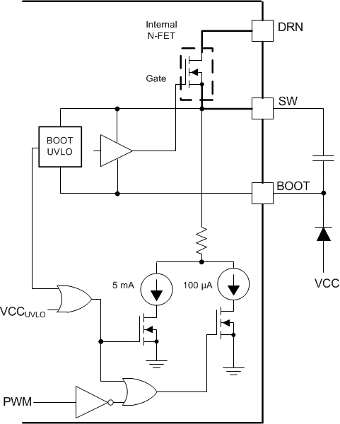 Figure 25. BOOT and PWM Pull-Downs
8.3.11 PWM (UVLO and Enable)
If PWM dimming or ON/OFF control is not needed in the application, the pin should be tied to VCC. The pin must be tied above 1 V if operation is desired.
PWM dimming can be achieved using the PWM pin. A signal above 1 V (typical) and below 900 mV (typical) when measured at the PWM pin should be used. Standard PWM frequency ranges can also be used (100 Hz to 2 kHz). When using higher frequencies the delays from PWM to gate turn ON and turn OFF can begin to limit the achievable duty cycle.
For example, the PWM to gate delay (turn on + turn off ≈ 100 ns) and the time to slew the switchnode up and down (approximately 100 ns) total approximately 200 ns.
For example, if a 10 kHz PWM frequency is desired having a period of 100 μs, the minimum duty cycle is 200 ns/100 μs = 0.2%. This is sometimes referred to as "500:1 dimming". As the PWM signal width becomes smaller, the converter ON and OFF time are eventually controlled by the PWM input signal directly. For example, if the PWM ON-time is shorter than the converter natural demanded ON-time, the PWM signal itself becomes the control signal for the high-side switch. The PWM pin activates a weak pulldown, as shown in Figure 25. Because the PWM pin is also UVLO (undervoltage lockout and device enable), when pulled low it is necessary to ensure the output is 100% OFF. The high-side FET driver has a small leakage path to the output. Although very small (<<100μA), theLEDs could glow if the current was not eliminated. The 100-μA (typical) pulldown is activated and held ON while PWM is low and ensures no light output.
8.3.11.1 Using PWM for UVLO (Undervoltage Lockout) Protection
When the PWM pin exceeds the 1-V (typical) threshold, the device activates a 100-mV (typical) fixed hysteresis and an adjustable hysteresis based on an internal current source (IPWM(uvlo-hys)). This functionality provides noise immunity to the PWM control and adjustability to the UVLO hysteresis. The two thresholds can be designed as described in the UVLO Programming Resistors section.
8.3.11.1.1 UVLO Programming Resistors
The value of resistors R2 and R3 establish the undervoltage lockout level as shown in Figure 26. Include a small level of capacitance (approximately 0.1 µF) at the UVLO pin for noise immunity. If the application does not require drop-out operation (operation when VIN approximates VLED) program a UVLO level allows no switching to occur until there is adequate input voltage available.
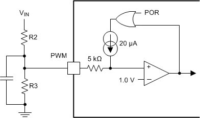 Figure 26. UVLO Programming Resistors
Select the desired amount of voltage hysteresis and the desired turn-ON threshold (VIN-RISE_THRESHOLD). Because of the small amount of fixed-voltage hysteresis and fixed-hysteresis current, some combinations of turn-ON and turn-OFF thresholds are not possible. If the calculation results in values that are zero or negative, the combinations selected are not possible. After selecting a turn-ON point and desired amount of voltage hysteresis (VHYST) use Equation 13 and Equation 14 to calculate R3 and R2.


8.3.11.2 Using PWM for Digitally Controlled Enable
If using the PWM pin as to provide and enable function, ensure the signal edge rate is adequate (< 100 ns) when measured at the device PWM pin to prevent the device from turning ON and turning OFF when the level transitions through the 1-V threshold region. If the edge is too slow or if the high level is not adequately above the 1-V threshold, a small capacitor may be required on the PWM pin to avoid multiple turn-ON and turn-OFF cycles when passing through this region.
8.3.11.3 UVLO: VIN, VCC and BOOT UVLO
The TPS92515 contains 3 internal under voltage lock-outs which must be satisfied for the device to operate: VIN UVLO ensures adequate voltage to power the high-side comparator. VCC UVLO ensures internal rails are adequate for the device to function, and BOOT UVLO ensures proper high-side FET operation and smooth dropout operation. All of the UVLO's operate independently and automatically. Under normal operation they do not require any specific user attention.
8.3.11.4 Analog and PWM Dimming - Normalized Results and Comparison
When the PWM applied signal is less than the switching cycle period and falls during an OFF-time it has no impact on the current for that cycle as the switch is already OFF. This situation can be avoided by increasing the switching frequency. Shunt FET PWM dimming avoids this issue. Current adjustment that maintains a constant ripple when shunted (see the OFF-Timer, Shunt FET Dimming or Shunted Output Condition section), creates a linear relation to the PWM shunt FET duty cycle and the average output current. Shunt FET PWM dimming can out-perform PWM dimming as characterized in Figure 27 through Figure 29, but is more complicated to implement.
Another impact on linearity can occur when using the analog dimming function. Discontinuous conduction mode (DCM) occurs when the inductor current reaches 0 A during each cycle,. When the device enters DCM, the output current is no longer the peak current minus half the ripple. The linear range can be extended by lowering the ripple, ΔIL-PP. If the system is being digitally controlled, the applied IADJ pin voltage can be adjusted when it is known the DCM operation occurs. In either case, a lower limit is eventually reached when the measured peak threshold voltage is approximately < 50 mV. At this point, the offset error becomes a significant portion of the peak current trip point voltage being measured.
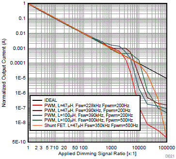
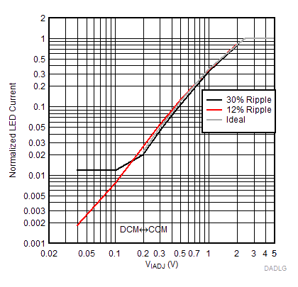
| VLED = 15 V | VIN = 55 V |
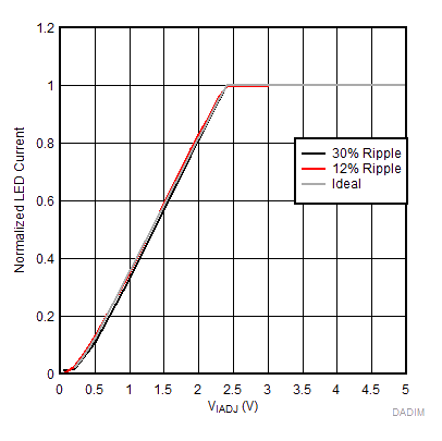
| VLED = 15 V | VIN = 55 V |
8.4 Device Functional Modes
This device has no additional functional modes.