SLUSCZ1 May 2017 TPS92518-Q1
PRODUCTION DATA.
- 1 Features
- 2 Applications
- 3 Description
- 4 Revision History
- 5 Pin Configuration and Functions
- 6 Specifications
- 7 Parameter Measurement Information
-
8 Detailed Description
- 8.1 Overview
- 8.2 Functional Block Diagram
- 8.3
Feature Description
- 8.3.1 General Operation
- 8.3.2 Important System Considerations: Off-Timer and Maximum Peak Threshold Values
- 8.3.3 Shunt FET or Matrix dimming: Maximum Off-timer Calculation
- 8.3.4 VIN and the VCC Internal Regulators
- 8.3.5 Output Enable Control Logic
- 8.3.6 BOOT Capacitor and BOOT UVLO
- 8.3.7 Drop-out Operation
- 8.3.8 Analog and PWM Dimming
- 8.3.9 VIN and CSPx Pin Configuration
- 8.3.10 Enable and Undervoltage Lock-out Configuration
- 8.3.11 Voltage Sampling and DAC Operation
- 8.3.12 Device Functional Modes
- 8.4 Serial Interface
- 8.5
Registers
- 8.5.1 CONTROL Register (Address = 00h) [reset = 00h]
- 8.5.2 STATUS (FAULT) Register (Address = 01h) [reset = 10h]
- 8.5.3 THERM_WARN_LMT Register (Address = 02h) [reset = 80h]
- 8.5.4 LED1_PKTH_DAC Register (Address = 03h) [reset = 80h]
- 8.5.5 LED2_PKTH_DAC Register (Address = 04h) [reset = 80h]
- 8.5.6 LED1_TOFF_DAC Register (Address = 05h) [reset = 80h]
- 8.5.7 LED2_TOFF_DAC Register (Address = 06h) [reset = 80h]
- 8.5.8 LED1_MAXOFF_DAC Register (Address = 07h) [reset = 80h]
- 8.5.9 LED2_MAXOFF_DAC Register (Address = 08h) [reset = 80h]
- 8.5.10 VTHERM Register (Address = 09h) [reset = 0h]
- 8.5.11 LED1_MOST_RECENT Register (Address = 0Ah) [reset = 0h]
- 8.5.12 LED1_LAST_ON Register (Address = 0Bh) [reset = 0h]
- 8.5.13 LED1_LAST_OFF Register (Address = 0Ch) [reset = 0h]
- 8.5.14 LED2_MOST_RECENT Register (Address = 0Dh) [reset = 0h]
- 8.5.15 LED2_LAST_ON Register (Address = 0Eh) [reset = 0h]
- 8.5.16 LED2_LAST_OFF Register (Address = 0Fh) [reset = 0h]
- 8.5.17 Reset Register (Address = 10h) [reset = 0h]
- 8.6 Programming
- 9 Application and Implementation
- 10Power Supply Recommendations
- 11Layout
- 12Device and Documentation Support
- 13Mechanical, Packaging, and Orderable Information
8.3.1.1 Constant Off-Time vs. Constant µs×V operation
Although commonly referred to as constant off-time, the off-time does vary with the output voltage in the standard TPS92518-Q1 configuration. This relation ensures constant peak-to-peak inductor current ripple (ΔIL-PP). Although not common, the VLEDx pin can be set to a fixed value to generate a truly constant off-time and limit changes in frequency, however current regulation degrades. To maintain regulation and a constant ripple over various output voltages, the converter off-time must become shorter or longer as VLEDx pin voltage changes. This results in a change in frequency. In this regard, the off-time register can be considered as a seconds-times-volts setting (s × V) for the converter. The TPS92518-Q1Electrical Characteristics table specification for off-time specifies a certain off time duration for a certain register value. The time is also dependent on the VLEDx pin voltage. For example, the off-time is specified at 4 µs for a VVLEDx= 30 V and LEDx_TOFF_DAC = 255. The internal analog circuitry operates to keep the ripple and µs·V (micro-second volt) product constant. If the LEDx voltage changes to 15 V, the off time adjusts to 8 µs. If the LEDx voltage changes to 60 V the off time adjusts to 2 µs, and so on.
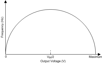
Two general cases can be examined: If the input voltage and output voltage are relatively constant, the frequency also remains constant. If either the input voltage or the output voltage changes, the frequency changes. For a fixed input voltage, the device operates at the maximum frequency at 50% duty cycle and the frequency reduces as the duty cycle becomes shorter or longer. A graphical representation is shown in Figure 17.
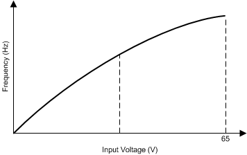
For a fixed output voltage (VVLEDx), the off-time stays fixed. The frequency then increases as the duty cycle becomes smaller with an increasing VIN voltage. This relation is shown in Figure 18.
 Figure 17. Frequency vs. LED Output Voltage. Fixed Input Voltage
 Figure 18. Frequency vs. Input Voltage. Fixed LED Voltage