SLUSCZ1 May 2017 TPS92518-Q1
PRODUCTION DATA.
- 1 Features
- 2 Applications
- 3 Description
- 4 Revision History
- 5 Pin Configuration and Functions
- 6 Specifications
- 7 Parameter Measurement Information
-
8 Detailed Description
- 8.1 Overview
- 8.2 Functional Block Diagram
- 8.3
Feature Description
- 8.3.1 General Operation
- 8.3.2 Important System Considerations: Off-Timer and Maximum Peak Threshold Values
- 8.3.3 Shunt FET or Matrix dimming: Maximum Off-timer Calculation
- 8.3.4 VIN and the VCC Internal Regulators
- 8.3.5 Output Enable Control Logic
- 8.3.6 BOOT Capacitor and BOOT UVLO
- 8.3.7 Drop-out Operation
- 8.3.8 Analog and PWM Dimming
- 8.3.9 VIN and CSPx Pin Configuration
- 8.3.10 Enable and Undervoltage Lock-out Configuration
- 8.3.11 Voltage Sampling and DAC Operation
- 8.3.12 Device Functional Modes
- 8.4 Serial Interface
- 8.5
Registers
- 8.5.1 CONTROL Register (Address = 00h) [reset = 00h]
- 8.5.2 STATUS (FAULT) Register (Address = 01h) [reset = 10h]
- 8.5.3 THERM_WARN_LMT Register (Address = 02h) [reset = 80h]
- 8.5.4 LED1_PKTH_DAC Register (Address = 03h) [reset = 80h]
- 8.5.5 LED2_PKTH_DAC Register (Address = 04h) [reset = 80h]
- 8.5.6 LED1_TOFF_DAC Register (Address = 05h) [reset = 80h]
- 8.5.7 LED2_TOFF_DAC Register (Address = 06h) [reset = 80h]
- 8.5.8 LED1_MAXOFF_DAC Register (Address = 07h) [reset = 80h]
- 8.5.9 LED2_MAXOFF_DAC Register (Address = 08h) [reset = 80h]
- 8.5.10 VTHERM Register (Address = 09h) [reset = 0h]
- 8.5.11 LED1_MOST_RECENT Register (Address = 0Ah) [reset = 0h]
- 8.5.12 LED1_LAST_ON Register (Address = 0Bh) [reset = 0h]
- 8.5.13 LED1_LAST_OFF Register (Address = 0Ch) [reset = 0h]
- 8.5.14 LED2_MOST_RECENT Register (Address = 0Dh) [reset = 0h]
- 8.5.15 LED2_LAST_ON Register (Address = 0Eh) [reset = 0h]
- 8.5.16 LED2_LAST_OFF Register (Address = 0Fh) [reset = 0h]
- 8.5.17 Reset Register (Address = 10h) [reset = 0h]
- 8.6 Programming
- 9 Application and Implementation
- 10Power Supply Recommendations
- 11Layout
- 12Device and Documentation Support
- 13Mechanical, Packaging, and Orderable Information
8.3.1.3 OFF Timer
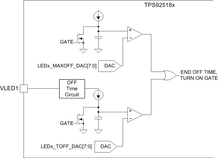
The converter Off-time is controlled via the LEDx_TOFF_DAC[7:0] register and VLEDx pin. The VLEDx pin voltage is converted to a current that charges an internal capacitor to a voltage set by the LEDx_TOFF_DAC creating a delay. Details of this circuit are shown in the Functional Block Diagram. Deriving the off-time from the output voltage creates a ramp representing the inductor current.
When the TPS92518-Q1 is first enabled (All UVLO levels are cleared) both timer capacitor pull-downs are disabled allowing voltage to increase on the internal timer capacitors. When either capacitor reaches the matching DAC control voltage, the high-side FET is turned on, starting a switching cycle. The maximum off-time timer is always dominant at start-up when the output is completely discharged or when shunt FET dimming and the shunt FET shunts the output for the required period.
 Figure 19. TPS92518-Q1 Simplified Internal Off-Timers Detail