SLUSCZ1 May   2017 TPS92518-Q1

PRODUCTION DATA.  

  1. Features
  2. Applications
  3. Description
    1.     Device Images
      1.      Simplified Schematic
  4. Revision History
  5. Pin Configuration and Functions
    1.     Pin Functions
  6. Specifications
    1. 6.1 Absolute Maximum Ratings
    2. 6.2 ESD Ratings
    3. 6.3 Recommended Operating Conditions
    4. 6.4 Thermal Information
    5. 6.5 Electrical Characteristics
    6. 6.6 Typical Characteristics
  7. Parameter Measurement Information
    1. 7.1 CSN Pin Falling Delay (tDEL)
    2. 7.2 Off-Timer (tOFF)
  8. Detailed Description
    1. 8.1 Overview
    2. 8.2 Functional Block Diagram
    3. 8.3 Feature Description
      1. 8.3.1  General Operation
        1. 8.3.1.1 Constant Off-Time vs. Constant µs×V operation
        2. 8.3.1.2 Output Equation
        3. 8.3.1.3 OFF Timer
          1. 8.3.1.3.1 Off-time and Maximum Off-time Calculations
      2. 8.3.2  Important System Considerations: Off-Timer and Maximum Peak Threshold Values
        1. 8.3.2.1 Peak Current Sense Comparator
        2. 8.3.2.2 Peak Current Threshold - LEDx _PKTH_DAC
        3. 8.3.2.3 Off-Time Thresholds - LEDx_TOFF_DAC and LEDx_MAXOFF_DAC
      3. 8.3.3  Shunt FET or Matrix dimming: Maximum Off-timer Calculation
        1. 8.3.3.1 Output Ringing and TPS92518-Q1 Protection
        2. 8.3.3.2 Live Peak and Off-Time Threshold Changes
      4. 8.3.4  VIN and the VCC Internal Regulators
      5. 8.3.5  Output Enable Control Logic
        1. 8.3.5.1 EN/UV2 - SPI Control Bypass
      6. 8.3.6  BOOT Capacitor and BOOT UVLO
      7. 8.3.7  Drop-out Operation
        1. 8.3.7.1 Early Drop-Out (Boot Capacitor Voltage >> VBOOT-UVLO)
        2. 8.3.7.2 Full Drop-Out (Boot Capacitor Voltage reaching VBOOT-UVLO)
        3. 8.3.7.3 Minimum BOOT Voltage and FET Control
        4. 8.3.7.4 BOOT Controlled internal Pull-Down
      8. 8.3.8  Analog and PWM Dimming
        1. 8.3.8.1 Dimming Methods
        2. 8.3.8.2 PWMx Pin Operation
        3. 8.3.8.3 PWM Dimming - Current Rise Performance
        4. 8.3.8.4 PWM and Analog Dimming - Linearity Limitations and Buck Converters
          1. 8.3.8.4.1 PWM:
          2. 8.3.8.4.2 ANALOG:
        5. 8.3.8.5 DCM Current Calculation
        6. 8.3.8.6 Current Sharing
      9. 8.3.9  VIN and CSPx Pin Configuration
      10. 8.3.10 Enable and Undervoltage Lock-out Configuration
      11. 8.3.11 Voltage Sampling and DAC Operation
        1. 8.3.11.1 ADC Control and LED Voltage Updating
      12. 8.3.12 Device Functional Modes
        1. 8.3.12.1 Analog Dimming
        2. 8.3.12.2 PWM Dimming
    4. 8.4 Serial Interface
      1. 8.4.1 Command Frame
      2. 8.4.2 Response Frame Formats
        1. 8.4.2.1 Read Response Frame Format
        2. 8.4.2.2 Write Response Frame Format
        3. 8.4.2.3 Write Error/POR Frame Format
        4. 8.4.2.4 SPI Error
    5. 8.5 Registers
      1. 8.5.1  CONTROL Register (Address = 00h) [reset = 00h]
        1. Table 3. CONTROL Register Field Descriptions
      2. 8.5.2  STATUS (FAULT) Register (Address = 01h) [reset = 10h]
        1. Table 4. STATUS Register Field Descriptions
      3. 8.5.3  THERM_WARN_LMT Register (Address = 02h) [reset = 80h]
        1. Table 5. THERM_WARN_LMT Register Field Descriptions
      4. 8.5.4  LED1_PKTH_DAC Register (Address = 03h) [reset = 80h]
        1. Table 6. LED1_PKTH_DAC Register Field Descriptions
      5. 8.5.5  LED2_PKTH_DAC Register (Address = 04h) [reset = 80h]
        1. Table 7. LED2_PKTH_DAC Register Field Descriptions
      6. 8.5.6  LED1_TOFF_DAC Register (Address = 05h) [reset = 80h]
        1. Table 8. LED1_TOFF_DAC Register Field Descriptions
      7. 8.5.7  LED2_TOFF_DAC Register (Address = 06h) [reset = 80h]
        1. Table 9. LED2_TOFF_DAC Register Field Descriptions
      8. 8.5.8  LED1_MAXOFF_DAC Register (Address = 07h) [reset = 80h]
        1. Table 10. LED1_MAXOFF_DAC Register Field Descriptions
      9. 8.5.9  LED2_MAXOFF_DAC Register (Address = 08h) [reset = 80h]
        1. Table 11. LED2_MAXOFF_DAC Register Field Descriptions
      10. 8.5.10 VTHERM Register (Address = 09h) [reset = 0h]
        1. Table 12. VTHERM Register Field Descriptions
      11. 8.5.11 LED1_MOST_RECENT Register (Address = 0Ah) [reset = 0h]
        1. Table 13. LED1_MOST_RECENT Register Field Descriptions
      12. 8.5.12 LED1_LAST_ON Register (Address = 0Bh) [reset = 0h]
        1. Table 14. LED1_LAST_ON Register Field Descriptions
      13. 8.5.13 LED1_LAST_OFF Register (Address = 0Ch) [reset = 0h]
        1. Table 15. LED1_LAST_OFF Register Field Descriptions
      14. 8.5.14 LED2_MOST_RECENT Register (Address = 0Dh) [reset = 0h]
        1. Table 16. LED2_MOST_RECENT Register Field Descriptions
      15. 8.5.15 LED2_LAST_ON Register (Address = 0Eh) [reset = 0h]
        1. Table 17. LED2_LAST_ON Register Field Descriptions
      16. 8.5.16 LED2_LAST_OFF Register (Address = 0Fh) [reset = 0h]
        1. Table 18. LED2_LAST_OFF Register Field Descriptions
      17. 8.5.17 Reset Register (Address = 10h) [reset = 0h]
        1. Table 19. Reset Register Field Descriptions
    6. 8.6 Programming
      1. 8.6.1 TPS92518-Q1 Register Typedef - Sample Code
      2. 8.6.2 Command Frame - Sample Code
      3. 8.6.3 SPI Read/Write - Sample Code
  9. Application and Implementation
    1. 9.1 Application Information
    2. 9.2 Typical Application
      1. 9.2.1 Design Requirements
      2. 9.2.2 Detailed Design Procedure
      3. 9.2.3 Application Curves
    3. 9.3 Dos and Don'ts
  10. 10Power Supply Recommendations
    1. 10.1 Input Source Direct from Battery
    2. 10.2 Input Source from a Boost Stage
  11. 11Layout
    1. 11.1 Layout Guidelines
    2. 11.2 Layout Example
  12. 12Device and Documentation Support
    1. 12.1 Receiving Notification of Documentation Updates
    2. 12.2 Community Resources
    3. 12.3 Trademarks
    4. 12.4 Electrostatic Discharge Caution
    5. 12.5 Glossary
  13. 13Mechanical, Packaging, and Orderable Information

封装选项

机械数据 (封装 | 引脚)
散热焊盘机械数据 (封装 | 引脚)
订购信息

ANALOG:

Another impact on linearity can occur when analog dimming (LEDx_PKTH_DAC threshold adjustment) and the inductor current becomes discontinuous. Discontinuous conduction mode (DCM) occurs when the inductor current reaches 0 A each off-time. When the device enters DCM, the output current is no longer the peak current minus half the ripple current (as shown in Figure 16) and is no longer a linear relationship between the LEDx_PKTH_DAC value and the average output current. The linear range can be extended by lowering the ripple, ΔIL-PP to extend the natural linear region of operation.
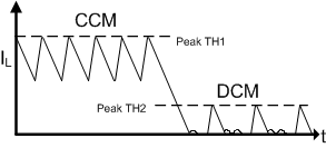
TPS92518-Q1 TPS92518_DCM.gifFigure 29. Analog Dimming Limitation

Another approach can be used by first analyzing the system operation. The point at which DCM is entered can be calculated as well as the average current value when in DCM. The micro-controller writing the LEDx_PKTH_DAC values can simply write alternate values in the DCM area to ensure net linear response to the LED average current. See DCM Current Calculationfor information on calculating the average current when in DCM.