SLUSCZ1 May 2017 TPS92518-Q1
PRODUCTION DATA.
- 1 Features
- 2 Applications
- 3 Description
- 4 Revision History
- 5 Pin Configuration and Functions
- 6 Specifications
- 7 Parameter Measurement Information
-
8 Detailed Description
- 8.1 Overview
- 8.2 Functional Block Diagram
- 8.3
Feature Description
- 8.3.1 General Operation
- 8.3.2 Important System Considerations: Off-Timer and Maximum Peak Threshold Values
- 8.3.3 Shunt FET or Matrix dimming: Maximum Off-timer Calculation
- 8.3.4 VIN and the VCC Internal Regulators
- 8.3.5 Output Enable Control Logic
- 8.3.6 BOOT Capacitor and BOOT UVLO
- 8.3.7 Drop-out Operation
- 8.3.8 Analog and PWM Dimming
- 8.3.9 VIN and CSPx Pin Configuration
- 8.3.10 Enable and Undervoltage Lock-out Configuration
- 8.3.11 Voltage Sampling and DAC Operation
- 8.3.12 Device Functional Modes
- 8.4 Serial Interface
- 8.5
Registers
- 8.5.1 CONTROL Register (Address = 00h) [reset = 00h]
- 8.5.2 STATUS (FAULT) Register (Address = 01h) [reset = 10h]
- 8.5.3 THERM_WARN_LMT Register (Address = 02h) [reset = 80h]
- 8.5.4 LED1_PKTH_DAC Register (Address = 03h) [reset = 80h]
- 8.5.5 LED2_PKTH_DAC Register (Address = 04h) [reset = 80h]
- 8.5.6 LED1_TOFF_DAC Register (Address = 05h) [reset = 80h]
- 8.5.7 LED2_TOFF_DAC Register (Address = 06h) [reset = 80h]
- 8.5.8 LED1_MAXOFF_DAC Register (Address = 07h) [reset = 80h]
- 8.5.9 LED2_MAXOFF_DAC Register (Address = 08h) [reset = 80h]
- 8.5.10 VTHERM Register (Address = 09h) [reset = 0h]
- 8.5.11 LED1_MOST_RECENT Register (Address = 0Ah) [reset = 0h]
- 8.5.12 LED1_LAST_ON Register (Address = 0Bh) [reset = 0h]
- 8.5.13 LED1_LAST_OFF Register (Address = 0Ch) [reset = 0h]
- 8.5.14 LED2_MOST_RECENT Register (Address = 0Dh) [reset = 0h]
- 8.5.15 LED2_LAST_ON Register (Address = 0Eh) [reset = 0h]
- 8.5.16 LED2_LAST_OFF Register (Address = 0Fh) [reset = 0h]
- 8.5.17 Reset Register (Address = 10h) [reset = 0h]
- 8.6 Programming
- 9 Application and Implementation
- 10Power Supply Recommendations
- 11Layout
- 12Device and Documentation Support
- 13Mechanical, Packaging, and Orderable Information
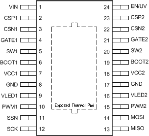
5 Pin Configuration and Functions
PWP Package
24-Pin HTTSOP
Top View

Pin Functions
| PINS | I/O | DESCRIPTION | |
|---|---|---|---|
| NAME | NO. | ||
| BOOT1 | 6 | I | Channel 1 bootstrap voltage input |
| BOOT2 | 19 | I | Channel 2 bootstrap voltage input |
| CSN1 | 3 | I | Channel 1 negative current sense input |
| CSN2 | 22 | I | Channel 2 negative current sense input |
| CSP1 | 2 | I | Channel 1 positive current sense input |
| CSP2 | 23 | I | Channel 2 positive current sense input |
| EN/UV | 24 | I | Device enable. If not configured as under voltage lock out or enable, tie to VCCx. Tie to >23.6V to bypass SPI communication and enable default register values. |
| GATE1 | 4 | O | Channel 1 gate drive output. Connect to FET gate |
| GATE2 | 21 | O | Channel 2 gate drive output. Connect to FET gate |
| GND | 8 | G | System ground |
| 17 | |||
| MISO | 13 | O | SPI data output |
| MOSI | 14 | I | SPI data input |
| PWM1 | 10 | I | Channel 1 PWM dimming input. Tie to VCCx if PWM pin control is not required. |
| PWM2 | 15 | I | Channel 2 PWM dimming input. Tie to VCCx if PWM pin control is not required. |
| SCK | 12 | I | SPI clock input |
| SSN | 11 | I | SPI slave select input |
| SW1 | 5 | I | Channel 1 switch node connection |
| SW2 | 20 | I | Channel 2 switch node connection |
| VCC1 | 7 | O | Channel 1 supply voltage output. May be used to power low current external circuits. See Application and Implementation section. |
| VCC2 | 18 | O | Channel 2 supply voltage output. May be used to power low current external circuits. See Application and Implementation section. |
| VIN | 1 | I | Device power supply voltage input. May be common to CSP1, CSP2 or an independent supply. |
| VLED1 | 9 | I | Channel 1 output voltage sense. |
| VLED2 | 16 | I | Channel 2 output voltage sense. |
| Exposed thermal pad | G | Connect to ground. Add vias to improve thermal performance. | |