SLUSCZ1 May 2017 TPS92518-Q1
PRODUCTION DATA.
- 1 Features
- 2 Applications
- 3 Description
- 4 Revision History
- 5 Pin Configuration and Functions
- 6 Specifications
- 7 Parameter Measurement Information
-
8 Detailed Description
- 8.1 Overview
- 8.2 Functional Block Diagram
- 8.3
Feature Description
- 8.3.1 General Operation
- 8.3.2 Important System Considerations: Off-Timer and Maximum Peak Threshold Values
- 8.3.3 Shunt FET or Matrix dimming: Maximum Off-timer Calculation
- 8.3.4 VIN and the VCC Internal Regulators
- 8.3.5 Output Enable Control Logic
- 8.3.6 BOOT Capacitor and BOOT UVLO
- 8.3.7 Drop-out Operation
- 8.3.8 Analog and PWM Dimming
- 8.3.9 VIN and CSPx Pin Configuration
- 8.3.10 Enable and Undervoltage Lock-out Configuration
- 8.3.11 Voltage Sampling and DAC Operation
- 8.3.12 Device Functional Modes
- 8.4 Serial Interface
- 8.5
Registers
- 8.5.1 CONTROL Register (Address = 00h) [reset = 00h]
- 8.5.2 STATUS (FAULT) Register (Address = 01h) [reset = 10h]
- 8.5.3 THERM_WARN_LMT Register (Address = 02h) [reset = 80h]
- 8.5.4 LED1_PKTH_DAC Register (Address = 03h) [reset = 80h]
- 8.5.5 LED2_PKTH_DAC Register (Address = 04h) [reset = 80h]
- 8.5.6 LED1_TOFF_DAC Register (Address = 05h) [reset = 80h]
- 8.5.7 LED2_TOFF_DAC Register (Address = 06h) [reset = 80h]
- 8.5.8 LED1_MAXOFF_DAC Register (Address = 07h) [reset = 80h]
- 8.5.9 LED2_MAXOFF_DAC Register (Address = 08h) [reset = 80h]
- 8.5.10 VTHERM Register (Address = 09h) [reset = 0h]
- 8.5.11 LED1_MOST_RECENT Register (Address = 0Ah) [reset = 0h]
- 8.5.12 LED1_LAST_ON Register (Address = 0Bh) [reset = 0h]
- 8.5.13 LED1_LAST_OFF Register (Address = 0Ch) [reset = 0h]
- 8.5.14 LED2_MOST_RECENT Register (Address = 0Dh) [reset = 0h]
- 8.5.15 LED2_LAST_ON Register (Address = 0Eh) [reset = 0h]
- 8.5.16 LED2_LAST_OFF Register (Address = 0Fh) [reset = 0h]
- 8.5.17 Reset Register (Address = 10h) [reset = 0h]
- 8.6 Programming
- 9 Application and Implementation
- 10Power Supply Recommendations
- 11Layout
- 12Device and Documentation Support
- 13Mechanical, Packaging, and Orderable Information
8.4 Serial Interface
The 4-wire control interface is compatible with the Serial Peripheral Interface (SPI) bus. The control bus consists of four signals: SSN, SCK, MOSI, and MISO. The SSN, SCK, and MOSI pins are TTL inputs into the TPS92518-Q1 while the MISO pin is an open-drain output. The SPI bus can be configured for both star-connect and daisy chain hardware connections.
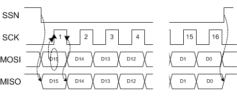
A bus transaction is initiated by a MCU on a falling edge of SSN. While SSN is low, the input data present on the MOSI pin is sampled on the rising edge of SCK, MSbit first. The output data is asserted on the MISO pin at the falling edge of SCK. The figure below shows the data transition and sampling edges of SCK.
A valid transfer requires a non-zero integer multiple of 16 SCK cycles (i.e., 16, 32, 48, etc.). If SSN is pulsed low and no SCK pulses are issued before SSN rises, a SPI error is reported. Similarly, if SSN is raised before the 16th rising edge of SCK, the transfer is aborted and a SPI error is reported. If SSN is held low after the 16th falling edge of SCK and additional SCK edges occur, the data continues to flow through the TPS92518-Q1 shift register and out the MISO pin. When SSN transitions from low-to-high, the internal digital block decodes the most recent 16 bits that were received prior to the SSN rising edge.
SSN must transition high only after a multiple of 16 SCK cycles for a transaction to be valid and not set the SPI error bit. In the case of a write transaction, the TPS92518-Q1 logic performs the requested operation when SSN transitions high. In the case of a read transaction, the read data is transferred during the next frame, regardless of whether a SPI error has occurred.
 Figure 33. SPI Data Format
The data bit on MOSI is shifted into an internal 16-bit shift register (MSbit first) while data is simultaneously shifted out the MISO pin. While SSN is high (bus idle), MISO is tri-stated by the open-drain driver. While SSN is low, MISO is driven according to the 16-bit data pattern being shifted out based on the prior received command. At the falling edge of SSN to begin a new transaction, MISO is driven to the MSbit of the outbound data, and is updated on each subsequent falling edge of SCK.
NOTE
The first MISO transition happens on the first falling edge AFTER the first rising edge of SCK.