ZHCSJM3B April   2019  – January 2020 TPS92613-Q1

PRODUCTION DATA.  

  1. 特性
  2. 应用
  3. 说明
    1.     Device Images
      1.      典型应用图
  4. 修订历史记录
  5. Pin Configuration and Functions
    1.     Pin Functions
  6. Specifications
    1. 6.1 Absolute Maximum Ratings
    2. 6.2 ESD Ratings
    3. 6.3 Recommended Operating Conditions
    4. 6.4 Thermal Information
    5. 6.5 Electrical Characteristics
    6. 6.6 Timing Requirements
    7. 6.7 Typical Characteristics
  7. Detailed Description
    1. 7.1 Overview
    2. 7.2 Functional Block Diagram
    3. 7.3 Feature Description
      1. 7.3.1 Power Supply
        1. 7.3.1.1 Power-On Reset (POR)
        2. 7.3.1.2 Low-Quiescent-Current
      2. 7.3.2 Constant-Current Driver
      3. 7.3.3 PWM Control
      4. 7.3.4 Supply Control
      5. 7.3.5 Diagnostics and Protection
        1. 7.3.5.1 Open-Circuit Detection
        2. 7.3.5.2 Short-to-GND Detection
        3. 7.3.5.3 Overtemperature Protection
        4. 7.3.5.4 DIAGEN
        5. 7.3.5.5 Low-Dropout Operation
      6. 7.3.6 FAULT Bus Output With One-Fails–All-Fail
      7. 7.3.7 Fault Table
    4. 7.4 Device Functional Modes
      1. 7.4.1 Undervoltage Lockout, V(SUPPLY) < V(POR_rising)
      2. 7.4.2 Normal Operation V(SUPPLY) ≥ 4.5 V
      3. 7.4.3 Low-Voltage Dropout Operation
      4. 7.4.4 Fault Mode
  8. Application and Implementation
    1. 8.1 Application Information
    2. 8.2 Typical Applications
      1. 8.2.1 Single-Channel LED Driver With Diagnostics
        1. 8.2.1.1 Design Requirements
        2. 8.2.1.2 Detailed Design Procedure
        3. 8.2.1.3 Application Curves
      2. 8.2.2 Single-Channel LED Driver With Heat Sharing
        1. 8.2.2.1 Design Requirements
        2. 8.2.2.2 Detailed Design Procedure
        3. 8.2.2.3 Application Curves
  9. Power Supply Recommendations
  10. 10Layout
    1. 10.1 Layout Guidelines
    2. 10.2 Layout Example
  11. 11器件和文档支持
    1. 11.1 文档支持
      1. 11.1.1 相关文档
    2. 11.2 接收文档更新通知
    3. 11.3 支持资源
    4. 11.4 商标
    5. 11.5 静电放电警告
    6. 11.6 Glossary
  12. 12机械、封装和可订购信息

封装选项

机械数据 (封装 | 引脚)
散热焊盘机械数据 (封装 | 引脚)
订购信息

Timing Requirements

MIN NOM MAX UNIT
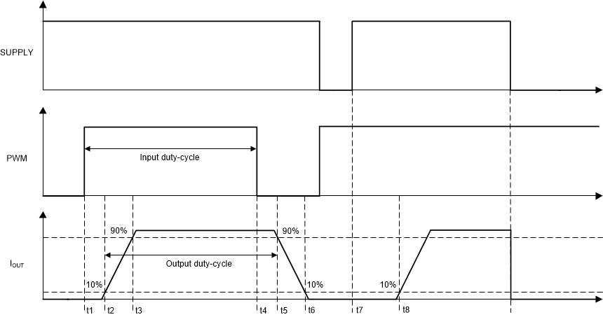
t(PWM_delay_rising) PWM rising edge delay, 50% PWM voltage to 10% of output current closed loop, t2 - t1 as shown in Figure 1 10 17 25 µs
t(PWM_delay_falling) PWM falling edge delay, 50% PWM voltage to 90% of output current open loop, t5 - t4 as shown in Figure 1 15 21 30 µs
t(DEVICE_STARTUP) SUPPLY rising edge to 10% output current at 200-mA set current and 14 V, t8 - t7 as shown in Figure 1 100 150 µs
t(OPEN_deg) LED-open fault-deglitch time 80 125 175 µs
t(SG_deg) Output short-to-ground detection deglitch time 80 125 175 µs
t(TSD_deg) Thermal over temperature deglitch timer 50 µs
t(Recover_deg) Fault recovery deglitch timer 8.5 16 25 µs
TPS92613-Q1 timing-02-slvsec4.gifFigure 1. Output Timing Diagram