ZHCSC40E February   2014  – May 2018 TPS92630-Q1

PRODUCTION DATA.  

  1. 特性
  2. 应用
  3. 说明
    1.     Device Images
      1.      典型应用原理图
  4. 修订历史记录
  5. 说明 (续)
  6. Pin Configuration and Functions
    1.     Pin Functions
  7. Specifications
    1. 7.1 Absolute Maximum Ratings
    2. 7.2 ESD Ratings
    3. 7.3 Recommended Operating Conditions
    4. 7.4 Thermal Information
    5. 7.5 Electrical Characteristics
    6. 7.6 Timing Requirements
    7. 7.7 Typical Characteristics
  8. Parameter Measurement Information
  9. Detailed Description
    1. 9.1 Overview
    2. 9.2 Functional Block Diagram
    3. 9.3 Feature Description
      1. 9.3.1 Constant LED-Current Setting
      2. 9.3.2 PWM Control
      3. 9.3.3 FAULT Diagnostics
      4. 9.3.4 Short-Circuit Detection
      5. 9.3.5 Open-Load Detection
      6. 9.3.6 Thermal Foldback
    4. 9.4 Device Functional Modes
      1. 9.4.1 Thermal Information
      2. 9.4.2 Operation With V(VIN) < 5 V (Minimum V(VIN))
      3. 9.4.3 Operation With 5 V < V(VIN) < 9 V (Lower-Than-Normal Automotive Battery Voltage)
  10. 10Applications and Implementation
    1. 10.1 Application Information
    2. 10.2 Typical Applications
      1. 10.2.1 Stoplight and Taillight Application With PWM Generator
        1. 10.2.1.1 Design Requirements
        2. 10.2.1.2 Detailed Design Procedure
          1. 10.2.1.2.1 Step-by-Step Design Procedure
            1. 10.2.1.2.1.1 R(REF)
            2. 10.2.1.2.1.2 Duty Cycle
            3. 10.2.1.2.1.3 Input and Output Capacitors
        3. 10.2.1.3 PWM Dimming Application Curve
      2. 10.2.2 Simple Stop-Light and Taillight Application
        1. 10.2.2.1 Design Requirements
        2. 10.2.2.2 Detailed Design Procedure
          1. 10.2.2.2.1 Step-by-Step Design Procedure
            1. 10.2.2.2.1.1 R(REF)
            2. 10.2.2.2.1.2 R(Stop)
            3. 10.2.2.2.1.3 Input and Output Capacitors
      3. 10.2.3 Parallel Connection
        1. 10.2.3.1 Design Requirements
        2. 10.2.3.2 Detailed Design Procedure
          1. 10.2.3.2.1 Step-by-Step Design Procedure
            1. 10.2.3.2.1.1 R(REF)
            2. 10.2.3.2.1.2 Input and Output Capacitors
      4. 10.2.4 Alternate Parallel Connection
        1. 10.2.4.1 Design Requirements
        2. 10.2.4.2 Detailed Design Procedure
          1. 10.2.4.2.1 Step-by-Step Design Procedure
            1. 10.2.4.2.1.1 R(REF)
            2. 10.2.4.2.1.2 Input and Output Capacitors
      5. 10.2.5 High-Side PWM Dimming
        1. 10.2.5.1 Design Requirements
        2. 10.2.5.2 Detailed Design Procedure
          1. 10.2.5.2.1 Step-by-Step Design Procedure
            1. 10.2.5.2.1.1 Ratio of Resistors, R1 / R2
            2. 10.2.5.2.1.2 R1 and R2 Selection
            3. 10.2.5.2.1.3 Input and Output Capacitors
  11. 11Power Supply Recommendations
  12. 12Layout
    1. 12.1 Layout Guidelines
    2. 12.2 Layout Example
  13. 13器件和文档支持
    1. 13.1 文档支持
      1. 13.1.1 相关文档
    2. 13.2 接收文档更新通知
    3. 13.3 社区资源
    4. 13.4 商标
    5. 13.5 静电放电警告
    6. 13.6 术语表
  14. 14机械、封装和可订购信息

封装选项

机械数据 (封装 | 引脚)
散热焊盘机械数据 (封装 | 引脚)
订购信息

Constant LED-Current Setting

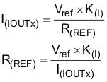
Control of the three LED output channels is through separate linear current regulators. A common external resistor sets the current in each channel. The device also features two current levels with external circuitry, intended for stop- and tail-light applications.

See Equation 1 on how to set the current:

Equation 1. TPS92630-Q1 eq1_Ioutx_slvsc76.gif