ZHCSMO6 June 2021 TPS92633
PRODUCTION DATA
- 1 特性
- 2 应用
- 3 说明
- 4 Revision History
- 5 Pin Configuration and Functions
- 6 Specifications
-
7 Detailed Description
- 7.1 Overview
- 7.2 Functional Block Diagram
- 7.3
Feature Description
- 7.3.1 Power Supply (SUPPLY)
- 7.3.2 Enable and Shutdown (EN)
- 7.3.3 Reference Current (IREF)
- 7.3.4 Constant-Current Output and Setting (INx)
- 7.3.5 Analog Current Control (ICTRL)
- 7.3.6 Thermal Sharing Resistor (OUTx and RESx)
- 7.3.7 PWM Control (PWMx)
- 7.3.8 Supply Control
- 7.3.9
Diagnostics
- 7.3.9.1 IREF Short-to-GND Detection
- 7.3.9.2 IREF Open Detection
- 7.3.9.3 LED Short-to-GND Detection
- 7.3.9.4 LED Open-Circuit Detection
- 7.3.9.5 Single LED Short-Circuit Detection (SLS_REF)
- 7.3.9.6 LED Open-Circuit and Single LED Short-Circuit Detection Enable (DIAGEN)
- 7.3.9.7 Low Dropout Operation
- 7.3.9.8 Over-Temperature Protection
- 7.3.10 FAULT Bus Output With One-Fails–All-Fail
- 7.3.11 FAULT Table
- 7.3.12 LED Fault Summary
- 7.3.13 IO Pins Inner Connection
- 7.4 Device Functional Modes
- 8 Application and Implementation
- 9 Power Supply Recommendations
- 10Layout
- 11Device and Documentation Support
- 12Mechanical, Packaging, and Orderable Information
7.3.7 PWM Control (PWMx)
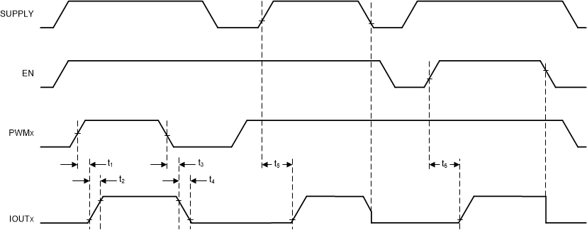
The pulse width modulation (PWM) input of the TPS92633 functions as enable for the output current. When the voltage applied on the PWM pin is higher than VIH(PWM), the relevant output current is enabled. When the voltage applied on PWM pin is lower than VIL(PWM), the output current is disabled as well as the diagnostic features. Besides output current enable and disable function, the PWM input of TPS92633 also supports adjustment of the average current output for brightness control when the frequency of applied PWM signal is higher than 100 Hz, which is out of visible frequency range of human eyes. TI recommends a 200-Hz PWM signal with 1% to 100% duty cycle input for brightness control. Please refer to Figure 7-5 for typical timming information and Figure 8-4 for typical PWM dimming application.
 Figure 7-5 Power On Sequency and PWM
Dimming Timing
Figure 7-5 Power On Sequency and PWM
Dimming TimingThe detailed information and value of each time period in Figure 7-5 is described in Timing Requirements.
The TPS92633 device has three total PWM input pins, PWM1, PWM2 and PWM3, to control each of current output channel independently. PWM1 input controls the output channel1 for both OUT1 and RES1, PWM2 input controls the output channel2 for both OUT2 and RES2, and PWM3 input controls the output channel3 for both OUT3 and RES3.