ZHCSMO6 June 2021 TPS92633
PRODUCTION DATA
- 1 特性
- 2 应用
- 3 说明
- 4 Revision History
- 5 Pin Configuration and Functions
- 6 Specifications
-
7 Detailed Description
- 7.1 Overview
- 7.2 Functional Block Diagram
- 7.3
Feature Description
- 7.3.1 Power Supply (SUPPLY)
- 7.3.2 Enable and Shutdown (EN)
- 7.3.3 Reference Current (IREF)
- 7.3.4 Constant-Current Output and Setting (INx)
- 7.3.5 Analog Current Control (ICTRL)
- 7.3.6 Thermal Sharing Resistor (OUTx and RESx)
- 7.3.7 PWM Control (PWMx)
- 7.3.8 Supply Control
- 7.3.9
Diagnostics
- 7.3.9.1 IREF Short-to-GND Detection
- 7.3.9.2 IREF Open Detection
- 7.3.9.3 LED Short-to-GND Detection
- 7.3.9.4 LED Open-Circuit Detection
- 7.3.9.5 Single LED Short-Circuit Detection (SLS_REF)
- 7.3.9.6 LED Open-Circuit and Single LED Short-Circuit Detection Enable (DIAGEN)
- 7.3.9.7 Low Dropout Operation
- 7.3.9.8 Over-Temperature Protection
- 7.3.10 FAULT Bus Output With One-Fails–All-Fail
- 7.3.11 FAULT Table
- 7.3.12 LED Fault Summary
- 7.3.13 IO Pins Inner Connection
- 7.4 Device Functional Modes
- 8 Application and Implementation
- 9 Power Supply Recommendations
- 10Layout
- 11Device and Documentation Support
- 12Mechanical, Packaging, and Orderable Information
7.3.9.4 LED Open-Circuit Detection
The TPS92633 device has LED open-circuit detection. The LED open-circuit detection monitors the output voltage when the current output is enabled. The LED open-circuit detection is only enabled when DIAGEN is HIGH.
The TPS92633 monitors dropout-voltage differences between the IN and OUT pins for each LED channel when PWM is HIGH. The voltage difference V(INx) – V(OUTx) is compared with the internal reference voltage V(OPEN_th_rising) to detect LED open-circuit incident. When V(OUTx) rises causing V(INx) – V(OUTx) less than the V(OPEN_th_rising) voltage and lasts longer the deglitch time of t(OPEN_deg), the device asserts an open-circuit fault. Once a LED open-circuit failure is detected, the internal constant-current sink pulls down the FAULT pin voltage. During the deglitch time period, when V(OUTx) falls and makes V(INx) – V(OUTx) larger than V(OPEN_th_falling), the deglitch timer is reset.
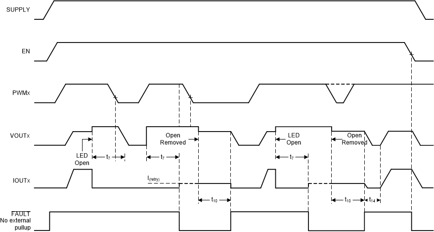
The TPS92633 shuts down the output current regulation for the faulty channel after LED open-circuit fault is detected. The device sources a small current I(Retry) from SUPPLY to OUT when DIAGEN input is logic High. Once the fault condition is removed, the device resumes normal operation and releases the FAULT pin. Figure 7-8 illustrates the timing for LED open-circuit detection, protection, retry and recovery.
 Figure 7-8 LED Open-Circuit Detection and
Recovery Timing Diagram
Figure 7-8 LED Open-Circuit Detection and
Recovery Timing DiagramThe detailed information and value of each time period in Figure 7-8 is described in Timing Requirements.