ZHCSMO6 June 2021 TPS92633
PRODUCTION DATA
- 1 特性
- 2 应用
- 3 说明
- 4 Revision History
- 5 Pin Configuration and Functions
- 6 Specifications
-
7 Detailed Description
- 7.1 Overview
- 7.2 Functional Block Diagram
- 7.3
Feature Description
- 7.3.1 Power Supply (SUPPLY)
- 7.3.2 Enable and Shutdown (EN)
- 7.3.3 Reference Current (IREF)
- 7.3.4 Constant-Current Output and Setting (INx)
- 7.3.5 Analog Current Control (ICTRL)
- 7.3.6 Thermal Sharing Resistor (OUTx and RESx)
- 7.3.7 PWM Control (PWMx)
- 7.3.8 Supply Control
- 7.3.9
Diagnostics
- 7.3.9.1 IREF Short-to-GND Detection
- 7.3.9.2 IREF Open Detection
- 7.3.9.3 LED Short-to-GND Detection
- 7.3.9.4 LED Open-Circuit Detection
- 7.3.9.5 Single LED Short-Circuit Detection (SLS_REF)
- 7.3.9.6 LED Open-Circuit and Single LED Short-Circuit Detection Enable (DIAGEN)
- 7.3.9.7 Low Dropout Operation
- 7.3.9.8 Over-Temperature Protection
- 7.3.10 FAULT Bus Output With One-Fails–All-Fail
- 7.3.11 FAULT Table
- 7.3.12 LED Fault Summary
- 7.3.13 IO Pins Inner Connection
- 7.4 Device Functional Modes
- 8 Application and Implementation
- 9 Power Supply Recommendations
- 10Layout
- 11Device and Documentation Support
- 12Mechanical, Packaging, and Orderable Information
7.3.6 Thermal Sharing Resistor (OUTx and RESx)
The TPS92633 device provides two current output paths for each channel. Current flows from the supply through the R(SNSx) resistor into the integrated current regulation circuit and to the LEDs through OUTx pin and RESx pin. The current output on both OUTx pin and RESx pin is independently regulated to achieve total required current output. The summed current of OUTx and RESx is equal to the current through the R(SNSx) resistor in the channel. The OUTx connects to anode of LEDs load in serial directly, however RESx connects to the LEDs through an external resistor to share part of the power dissipation and reduce the thermal accumulation in TPS92633.
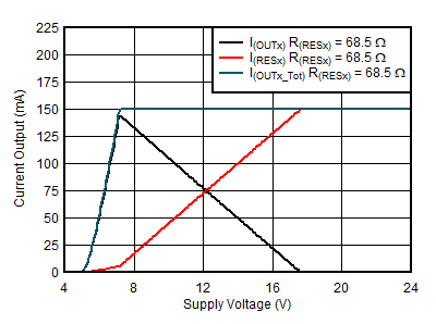
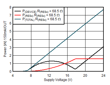
The integrated independent current regulation in TPS92633 dynamically adjusts the output current on both OUTx and RESx output to maintain the stable summed current for LED. The TPS92633 always regulates the current output to the RESx pin as much as possible until the RESx current path is saturated, and the rest of required current is regulated from the OUTx. As a result, the most of the current to LED outputs through the RESx pin when the voltage dropout is relatively high between SUPPLY and LED required total forward voltage. In the opposite case, the most of the current to LED outputs through the OUTx pin when the voltage headroom is relatively low between SUPPLY and LED required forward voltage. Figure 7-3 and Figure 7-4 shows the curve of current and power dissipation distributor depending on supply voltage when R(RESx) is 68.5 Ω.
 Figure 7-3 Output Current Distribution vs
Supply Voltage
 Figure 7-4 Power Dissipation vs Supply
Voltage