ZHCSEM9 December 2015 TPS92691 , TPS92691-Q1
PRODUCTION DATA.
- 1 特性
- 2 应用
- 3 说明
- 4 修订历史记录
- 5 Pin Configuration and Functions
- 6 Specifications
-
7 Detailed Description
- 7.1 Overview
- 7.2 Functional Block Diagram
- 7.3
Feature Description
- 7.3.1 Internal Regulator and Undervoltage Lockout (UVLO)
- 7.3.2 Oscillator
- 7.3.3 Gate Driver
- 7.3.4 Rail-to-Rail Current Sense Amplifier
- 7.3.5 Transconductance Error Amplifier
- 7.3.6 Switch Current Sense and Internal Slope Compensation
- 7.3.7 Analog Adjust Input
- 7.3.8 PWM Input and Series Dimming FET Gate Driver Output
- 7.3.9 Soft-Start
- 7.3.10 Current Monitor Output
- 7.3.11 Overvoltage Protection
- 7.3.12 Thermal Protection
- 7.4 Device Functional Modes
-
8 Application and Implementation
- 8.1
Application Information
- 8.1.1 Duty Cycle Considerations
- 8.1.2 Inductor Selection
- 8.1.3 Output Capacitor Selection
- 8.1.4 Input Capacitor Selection
- 8.1.5 Main Power MOSFET Selection
- 8.1.6 Rectifier Diode Selection
- 8.1.7 LED Current Programming
- 8.1.8 Switch Current Sense Resistor and Slope Compensation
- 8.1.9 Feedback Compensation
- 8.1.10 Soft-Start
- 8.1.11 Overvoltage Protection
- 8.1.12 PWM Dimming Considerations
- 8.2
Typical Applications
- 8.2.1
Typical Boost LED Driver
- 8.2.1.1 Design Requirements
- 8.2.1.2
Detailed Design Procedure
- 8.2.1.2.1 Calculating Duty Cycle
- 8.2.1.2.2 Setting Switching Frequency
- 8.2.1.2.3 Inductor Selection
- 8.2.1.2.4 Output Capacitor Selection
- 8.2.1.2.5 Input Capacitor Selection
- 8.2.1.2.6 Main N-Channel MOSFET Selection
- 8.2.1.2.7 Rectifying Diode Selection
- 8.2.1.2.8 Programming LED Current
- 8.2.1.2.9 Setting Switch Current Limit and Slope Compensation
- 8.2.1.2.10 Deriving Compensator Parameters
- 8.2.1.2.11 Setting Start-up Duration
- 8.2.1.2.12 Setting Overvoltage Protection Threshold
- 8.2.1.2.13 PWM Dimming Considerations
- 8.2.1.3 Application Curves
- 8.2.2
Typical Buck-Boost LED Driver
- 8.2.2.1 Design Requirements
- 8.2.2.2
Detailed Design Procedure
- 8.2.2.2.1 Calculating Duty Cycle
- 8.2.2.2.2 Setting Switching Frequency
- 8.2.2.2.3 Inductor Selection
- 8.2.2.2.4 Output Capacitor Selection
- 8.2.2.2.5 Input Capacitor Selection
- 8.2.2.2.6 Main N-Channel MOSFET Selection
- 8.2.2.2.7 Rectifier Diode Selection
- 8.2.2.2.8 Setting Switch Current Limit and Slope Compensation
- 8.2.2.2.9 Programming LED Current
- 8.2.2.2.10 Deriving Compensator Parameters
- 8.2.2.2.11 Setting Startup Duration
- 8.2.2.2.12 Setting Overvoltage Protection Threshold
- 8.2.2.2.13 PWM Dimming Consideration
- 8.2.2.3 Application Curves
- 8.2.1
Typical Boost LED Driver
- 8.1
Application Information
- 9 Power Supply Recommendations
- 10Layout
- 11器件和文档支持
- 12机械、封装和可订购信息
6 Specifications
6.1 Absolute Maximum Ratings
over operating free-air temperature range (unless otherwise noted)(1)(2)| MIN | MAX | UNIT | ||
|---|---|---|---|---|
| Input voltage | VIN, CSP, CSN | –0.3 | 65 | V |
| IADJ, IS, PWM, RT/SYNC | –0.3 | 8.8 | V | |
| OVP, SS | –0.3 | 5.5 | V | |
| CSP to CSN(3), PGND | –0.3 | 0.3 | V | |
| Output voltage(4) | VCC, GATE, DDRV | –0.3 | 8.8 | V |
| COMP | –0.3 | 5.0 | V | |
| Source current | IMON | — | 100 | µA |
| GATE, DDRV (Pulsed <20 ns) | — | 500 | mA | |
| Sink current | GATE, DDRV (Pulsed <20 ns) | — | 500 | mA |
| Operating junction temperature, TJ | –40 | 140 | °C | |
| Storage temperature, Tstg | 150 | °C | ||
(1) Stresses beyond those listed under Absolute Maximum Ratings may cause permanent damage to the device. These are stress ratings only, which do not imply functional operation of the device at these or any other conditions beyond those indicated under Recommended Operating Conditions. Exposure to absolute-maximum-rated conditions for extended periods may affect device reliability.
(2) All voltages are with respect to AGND unless otherwise noted
(3) Continuous sustaining voltage
(4) All output pins are not specified to have an external voltage applied.
6.2 ESD Ratings
| VALUE | UNIT | ||||
|---|---|---|---|---|---|
| TPS92691-Q1 IN PWP (HTSSOP) PACKAGE | |||||
| V(ESD) | Electrostatic discharge | Human-body model (HBM), per AEC Q100-002, all pins(1) | ±2000 | V | |
| Charged-device model (CDM), per AEC Q100-011 | All pins except 1, 8, 9, and 16 | ±500 | |||
| Pins 1, 8, 9, and 16 | ±750 | ||||
| TPS92691 IN PWP (HTSSOP) PACKAGE | |||||
| V(ESD) | Electrostatic discharge | Human-body model (HBM), per ANSI/ESDA/JEDEC JS-001, all pins(2) | ±2000 | V | |
| Charged-device model (CDM), per JEDEC specification JESD22-C101, all pins(3) | ±500 | ||||
(1) AEC Q100-002 indicates that HBM stressing shall be in accordance with the ANSI/ESDA/JEDEC JS-001 specification.
(2) JEDEC document JEP155 states that 500-V HBM allows safe manufacturing with a standard ESD control process.
(3) JEDEC document JEP157 states that 250-V CDM allows safe manufacturing with a standard ESD control process.
6.3 Recommended Operating Conditions
over operating free-air temperature range (unless otherwise noted)| MIN | NOM | MAX | UNIT | ||
|---|---|---|---|---|---|
| VIN | Supply input voltage | 6.5 | 14 | 65 | V |
| VIN, crank | Supply input, battery crank voltage | 4.5 | V | ||
| VCSP, VCSN | Current sense common mode | 0 | 60 | V | |
| ƒSW | Switching frequency | 80 | 700 | kHz | |
| ƒSYNC | SYNC frequency | 0.8 × ƒsw | 1.2 × ƒSW | kHz | |
| VIADJ | Current reference voltage | 0.14 | VIADJ(CLAMP) | V | |
| TA | Operating ambient temperature | –40 | 125 | °C | |
6.4 Thermal Information
| THERMAL METRIC(1) | TPS92691/-Q1 | UNIT | |
|---|---|---|---|
| PWP (HTSSOP) | |||
| 16 PINS | |||
| RθJA | Junction-to-ambient thermal resistance | 40.8 | °C/W |
| RθJC(top) | Junction-to-case (top) thermal resistance | 26.1 | °C/W |
| RθJB | Junction-to-board thermal resistance | 22.2 | °C/W |
| ψJT | Junction-to-top characterization parameter | 0.8 | °C/W |
| ψJB | Junction-to-board characterization parameter | 22.0 | °C/W |
| RθJC(bot) | Junction-to-case (bottom) thermal resistance | 2.3 | °C/W |
(1) For more information about traditional and new thermal metrics, see the Semiconductor and IC Package Thermal Metrics application report, SPRA953.
6.5 Electrical Characteristics
TJ = –40°C to 140°C, VIN = 14 V, VIADJ = 2.2 V, CVCC = 1 µF, CCOMP = 2.2 nF, RCS = 100 mΩ, RT = 20 kΩ, VPWM = 5 V, no load on GATE and DDRV (unless otherwise noted)(1)| PARAMETER | TEST CONDITIONS | MIN | TYP | MAX | UNIT | |
|---|---|---|---|---|---|---|
| INPUT VOLTAGE (VIN) | ||||||
| VDO | LDO dropout voltage | ICC = 20 mA, VIN = 5 V | 300 | mV | ||
| BIAS SUPPLY (VCC) | ||||||
| VCC(REG) | Regulation voltage | No load | 7.0 | 7.5 | 8.0 | V |
| VCC(UVLO) | Supply undervoltage protection | VCC rising threshold, VIN = 8 V | 4.1 | 4.35 | V | |
| VCC falling threshold, VIN = 8 V | 3.75 | 4.0 | V | |||
| Hysteresis | 100 | mV | ||||
| ICC(LIMIT) | Supply current limit | VCC = 0 V | 26 | 38 | 46 | mA |
| ICC(STBY) | Supply stand-by current | VPWM = 0 V | 1.8 | 2.1 | mA | |
| ICC(SW) | Supply switching current | VCC = 7.5 V, CGATE = 1 nF | 5.1 | 6.6 | mA | |
| OSCILLATOR (RT/SYNC) | ||||||
| ƒSW | Switching frequency | RT = 40 kΩ | 165 | 200 | 230 | kHz |
| RT = 20 kΩ | 327 | 390 | 448 | kHz | ||
| VRT | RT output voltage | 1 | V | |||
| VSYNC | SYNC rising threshold | VRT/SYNC rising | 2.7 | 3.1 | V | |
| SYNC falling threshold | VRT/SYNC falling | 1.8 | 2 | V | ||
| tSYNC(MIN) | Minimum SYNC clock pulse width | 100 | ns | |||
| GATE DRIVER (GATE) | ||||||
| RGH | Gate driver high side resistance | IGATE = –10 mA | 5.4 | 11.2 | Ω | |
| RGL | Gate driver low side resistance | IGATE = 10 mA | 4.3 | 10.5 | Ω | |
| CURRENT SENSE (IS) | ||||||
| VIS(LIMIT) | Current limit threshold | 497 | 525 | 550 | mV | |
| tIS(BLANK) | Leading edge blanking time | 103 | 150 | 188 | ns | |
| tIS(FAULT) | Current limit fault time | 35 | µs | |||
| tILMT(DLY) | IS to GATE propagation delay | VIS pulsed from 0 to 1 V | 100 | ns | ||
| PWM COMPARATOR AND SLOPE COMPENSATION | ||||||
| DMAX | Maximum duty cycle | 90.4% | 93% | 94.7% | ||
| VLV | IS to COMP level shift voltage | No slope compensation added | 1.17 | 1.5 | 1.8 | V |
| VSL | Slope compensation | D = DMAX (with max slope compensation) | 200 | mV | ||
| ILV | IS level shift bias current | No slope compensation added | 25 | µA | ||
| ILV + ISL | IS level shift source current | D = DMAX (with max slope compensation) | 115 | µA | ||
| CURRENT SENSE AMPLIFIER (CSP, CSN) | ||||||
| VCS(offset) | Cumulative offset voltage at VCSP = 60 V and V(CSP-CSN) = 150 mV, referred to current sense input | –40°C ≤ TJ ≤ 140°C | –5.2 | 5.9 | mV | |
| 25°C ≤ TJ ≤ 140°C | –4.4 | 4.6 | mV | |||
| Cumulative offset voltage at VCSP = 60 V and V(CSP-CSN) = 10 mV, referred to current sense input | –40°C ≤ TJ ≤ 140°C | –3.5 | 5.0 | mV | ||
| 25°C ≤ TJ ≤ 140°C | -2.8 | 4.0 | mV | |||
| Cumulative offset voltage at VCSN = 0 V and V(CSP-CSN) = 150 mV, referred to current sense input | –40°C ≤ TJ ≤ 140°C | –5.9 | 6.7 | mV | ||
| 25°C ≤ TJ ≤ 140°C | -4.7 | 5.0 | mV | |||
| Cumulative offset voltage at VCSN = 0 V and V(CSP-CSN) = 10 mV, referred to current sense input | –40°C ≤ TJ ≤ 140°C | –2.3 | 3.2 | mV | ||
| 25°C ≤ TJ ≤ 140°C | –1.7 | 2.6 | mV | |||
| CS(BW) | Current sense unity gain bandwidth | 500 | kHz | |||
| ICS(BIAS) | CSP, CSN bias current | VCSP, CSN = 60 V | 4 | µA | ||
| CURRENT MONITOR (IMON) | ||||||
| VIMON(CLP) | IMON output voltage clamp | 3.2 | 3.7 | 4.2 | V | |
| VIMON(OS) | IMON buffer offset voltage | –11.4 | –1.6 | 7.3 | mV | |
| ANALOG ADJUST (IADJ) | ||||||
| VIADJ(CLP) | IADJ internal clamp voltage | IIADJ = 1 µA | 2.27 | 2.42 | 2.55 | V |
| IIADJ(BIAS) | IADJ input bias current | VIADJ < 2.2 V | 90 | nA | ||
| RIADJ(LMT) | IADJ current limiting series resistor | VIADJ > 2.6 V | 12 | kΩ | ||
| ERROR AMPLIFIER (COMP) | ||||||
| gM | Transconductance | 121 | µA/V | |||
| ICOMP(SRC) | COMP current source capacity | VIADJ = 1.4 V, V(CSP-CSN) = 0 V | 130 | µA | ||
| ICOMP(SINK) | COMP current sink capacity | VIADJ = 0 V, V(CSP-CSN) = 0.1 V | 130 | µA | ||
| EA(BW) | Error amplifier bandwidth | –3 dB | 5 | MHz | ||
| VCOMP(RST) | COMP pin reset voltage | 100 | mV | |||
| RCOMP(DCH) | COMP discharge FET resistance | 246 | Ω | |||
| SOFT-START (SS) | ||||||
| ISS | Soft-start source current | 7 | 10 | 12.8 | µA | |
| VSS(RST) | Soft-start pin reset voltage | 25 | mV | |||
| RSS(DCH) | SS discharge FET resistance | 260 | Ω | |||
| OVERVOLTAGE PROTECTION (OVP) | ||||||
| VOVP(THR) | OVP detection threshold | 1.18 | 1.24 | 1.31 | V | |
| IOVP(HYS) | OVP hysteresis current | 12 | 20 | 27.5 | µA | |
| PWM INPUT (PWM) | ||||||
| VPWM(HIGH) | Schmitt trigger logic level (high threshold) | 2.5 | 2.7 | V | ||
| VPWM(LOW) | Schmitt trigger logic level (low threshold) | 2.0 | 2.3 | V | ||
| RPWM(PD) | PWM pulldown resistance | 1 | MΩ | |||
| tDLY(RISE) | PWM to DDRV rising delay | 54 | ns | |||
| tDLY(FALL) | PWM to DDRV falling delay | 72 | ns | |||
| PWM GATE DRIVE OUTPUT (DDRV) | ||||||
| RDH | DDRV high-side resistance | 6.1 | 12.8 | Ω | ||
| RDL | DDRV low-side resistance | 5.2 | 11.4 | Ω | ||
| THERMAL SHUTDOWN | ||||||
| Thermal shutdown temperature | 175 | °C | ||||
| Thermal shutdown hysteresis | 25 | °C | ||||
(1) All voltages are with respect to AGND unless otherwise noted
6.6 Typical Characteristics
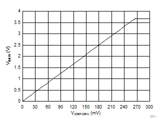
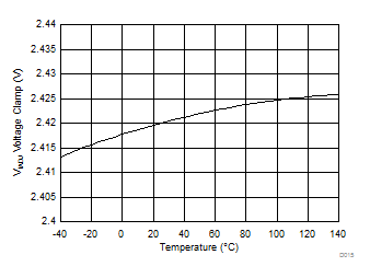
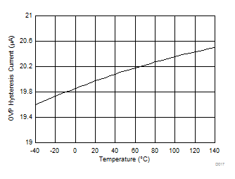
TA = 25°C, VIN = 14 V, VIADJ = 2.2 V, CVCC = 1 µF, CCOMP = 2.2 nF, RCS = 100 mΩ, RT = 20 kΩ, VPWM = 5 V, no load on GATE and DDRV (unless otherwise noted)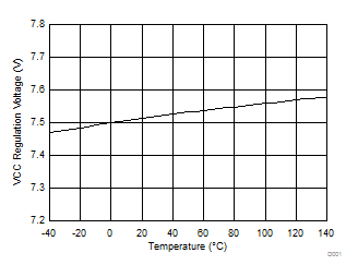
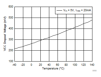
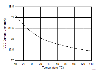


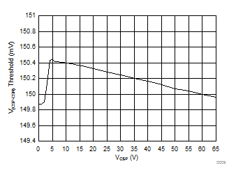
| VIADJ = 2.1 V |
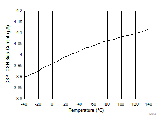
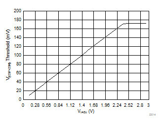

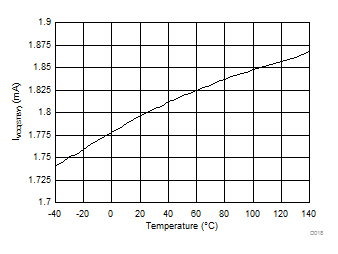
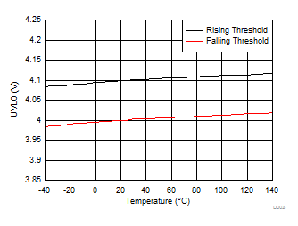


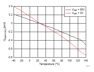
| VIADJ = 2.1 V |
