ZHCSEM9 December 2015 TPS92691 , TPS92691-Q1
PRODUCTION DATA.
- 1 特性
- 2 应用
- 3 说明
- 4 修订历史记录
- 5 Pin Configuration and Functions
- 6 Specifications
-
7 Detailed Description
- 7.1 Overview
- 7.2 Functional Block Diagram
- 7.3
Feature Description
- 7.3.1 Internal Regulator and Undervoltage Lockout (UVLO)
- 7.3.2 Oscillator
- 7.3.3 Gate Driver
- 7.3.4 Rail-to-Rail Current Sense Amplifier
- 7.3.5 Transconductance Error Amplifier
- 7.3.6 Switch Current Sense and Internal Slope Compensation
- 7.3.7 Analog Adjust Input
- 7.3.8 PWM Input and Series Dimming FET Gate Driver Output
- 7.3.9 Soft-Start
- 7.3.10 Current Monitor Output
- 7.3.11 Overvoltage Protection
- 7.3.12 Thermal Protection
- 7.4 Device Functional Modes
-
8 Application and Implementation
- 8.1
Application Information
- 8.1.1 Duty Cycle Considerations
- 8.1.2 Inductor Selection
- 8.1.3 Output Capacitor Selection
- 8.1.4 Input Capacitor Selection
- 8.1.5 Main Power MOSFET Selection
- 8.1.6 Rectifier Diode Selection
- 8.1.7 LED Current Programming
- 8.1.8 Switch Current Sense Resistor and Slope Compensation
- 8.1.9 Feedback Compensation
- 8.1.10 Soft-Start
- 8.1.11 Overvoltage Protection
- 8.1.12 PWM Dimming Considerations
- 8.2
Typical Applications
- 8.2.1
Typical Boost LED Driver
- 8.2.1.1 Design Requirements
- 8.2.1.2
Detailed Design Procedure
- 8.2.1.2.1 Calculating Duty Cycle
- 8.2.1.2.2 Setting Switching Frequency
- 8.2.1.2.3 Inductor Selection
- 8.2.1.2.4 Output Capacitor Selection
- 8.2.1.2.5 Input Capacitor Selection
- 8.2.1.2.6 Main N-Channel MOSFET Selection
- 8.2.1.2.7 Rectifying Diode Selection
- 8.2.1.2.8 Programming LED Current
- 8.2.1.2.9 Setting Switch Current Limit and Slope Compensation
- 8.2.1.2.10 Deriving Compensator Parameters
- 8.2.1.2.11 Setting Start-up Duration
- 8.2.1.2.12 Setting Overvoltage Protection Threshold
- 8.2.1.2.13 PWM Dimming Considerations
- 8.2.1.3 Application Curves
- 8.2.2
Typical Buck-Boost LED Driver
- 8.2.2.1 Design Requirements
- 8.2.2.2
Detailed Design Procedure
- 8.2.2.2.1 Calculating Duty Cycle
- 8.2.2.2.2 Setting Switching Frequency
- 8.2.2.2.3 Inductor Selection
- 8.2.2.2.4 Output Capacitor Selection
- 8.2.2.2.5 Input Capacitor Selection
- 8.2.2.2.6 Main N-Channel MOSFET Selection
- 8.2.2.2.7 Rectifier Diode Selection
- 8.2.2.2.8 Setting Switch Current Limit and Slope Compensation
- 8.2.2.2.9 Programming LED Current
- 8.2.2.2.10 Deriving Compensator Parameters
- 8.2.2.2.11 Setting Startup Duration
- 8.2.2.2.12 Setting Overvoltage Protection Threshold
- 8.2.2.2.13 PWM Dimming Consideration
- 8.2.2.3 Application Curves
- 8.2.1
Typical Boost LED Driver
- 8.1
Application Information
- 9 Power Supply Recommendations
- 10Layout
- 11器件和文档支持
- 12机械、封装和可订购信息
7 Detailed Description
7.1 Overview
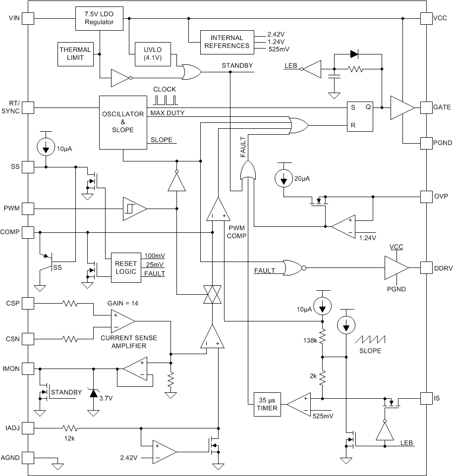
The TPS92691/-Q1 wide input range (4.5 V to 65 V) controller features all of the functions necessary to implement a highly efficient and compact LED driver based on step-up or step-down converter topologies. The device implements a fixed-frequency, peak current mode control technique to achieve a constant current output, ideal for driving a single string of series-connected LEDs. The integrated low input offset, rail-to-rail current sense amplifier supports a wide range of output voltages (0 V to 65 V) and is capable of powering an LED string consisting of 1 to more than 20 white LEDs. The controller is compatible with either high- or low-side current shunt sensing technique, based on the LED configuration and driver topology. The LED current sense threshold, set by the analog adjust input, IADJ, provides the capability to analog (amplitude) dim over a linear range of 15:1 by varying the voltage, VIADJ, from 140 mV to 2.25 V. The IADJ input provides the means to externally program LED current and facilitates calibration, brightness correction, and thermal management of the LEDs. High resolution and linear dimming response is achieved by varying the duty cycle of LED current based on the PWM input. The PWM input directly controls the GATE and DDRV drive outputs, controls the internal oscillator, and enables high-speed PWM dimming with over 1000:1 contrast ratio when using an external MOSFET placed in series with the LED load. The current monitor output, IMON, reports the instantaneous status of LED current measured by the rail-to-rail current sense amplifier. This feature is incorporated to indicate LED short and open-circuit failures and enables cable harness fault detection independent of LED driver topology. Other fault protection features include cycle-by-cycle current limiting, hysteresis-based overvoltage protection, VCC undervoltage protection, thermal shutdown, and remote shutdown capability by pulling down the SS pin.
7.2 Functional Block Diagram

7.3 Feature Description
7.3.1 Internal Regulator and Undervoltage Lockout (UVLO)
The IC incorporates a 65-V input VIN rated linear regulator to generate the 7.5 V (typ) VCC bias supply and other internal reference voltages. The VCC output is monitored to implement UVLO protection. The device is enabled when VCC exceeds the 4.1-V (typ) threshold and is disabled when VCC drops below the 4.0-V (typ) threshold. The UVLO comparator provides 0.1 V of hysteresis to avoid chatter during transitions. The UVLO thresholds are internally fixed and cannot be adjusted. The supply current, ICC, is limited to 26 mA minimum to protect the device under VCC pin short-circuit conditions. The VCC supply powers the internal circuitry and N-channel gate driver outputs, GATE, and DDRV. Place a bypass capacitor in the range of 2.2 µF to 4.7 µF across the VCC output and PGND to ensure proper operation. The regulator operates in dropout when input voltage VIN falls below 7.5 V forcing VCC to be lower than VIN by 300 mV for a 20-mA supply current. The VCC is a regulated output of the internal regulator and is not recommended to be driven from an external power supply.
7.3.2 Oscillator
The TPS92691/-Q1 switching frequency is programmable by a single external resistor connected between the RT/SYNC pin and the AGND pin. To set a desired frequency, ƒSW (Hz), the resistor value can be calculated from Equation 1.

Figure 6 shows a graph of switching frequency versus resistance, RT. TI recommends a switching frequency setting between 80 kHz and 700 kHz for optimal performance over input and output voltage operating range and for best efficiency. Operation at higher switching frequencies requires careful selection of N-channel MOSFET characteristics and should take into consideration additional switching losses and junction temperature rise.
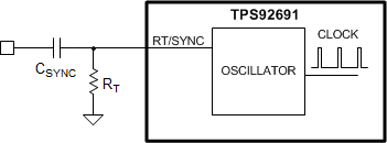
 Figure 19. Oscillator Synchronization Through AC Coupling
The internal oscillator can be synchronized by AC coupling an external clock pulse to RT/SYNC pin as shown in Figure 19. The positive going synchronization clock at the RT pin must exceed the RT sync threshold and the negative going synchronization clock at the RT pin must exceed the RT sync falling threshold to trip the internal synchronization pulse detector. TI recommends that the frequency of the external synchronization pulse is within ±20% of the internal oscillator frequency programmed by the RT resistor. TI recommends a minimum coupling capacitor of 100 nF and typical pulse width of 100 ns for proper synchronization. In the case where external synchronization clock is lost the internal oscillator takes control of the switching rate based on the RT resistor to maintain output current regulation. The RT resistor is always required whether the oscillator is free running or externally synchronized.
7.3.3 Gate Driver
The TPS92691/-Q1 contains a N-channel gate driver that switches the output VGATE between VCC and PGND. A peak source and sink current of 500 mA allows controlled slew-rate of the MOSFET gate and drain node voltages, limiting the conducted and radiated EMI generated by switching. The gate driver supply current ICC(GATE) depends on the total gate drive charge (QG) of the MOSFET and the operating frequency of the converter, ƒSW,  . TI recommends a MOSFET with a low gate charge specification to limit the junction temperature rise and switch transition losses.
While choosing the N-channel MOSFET device, consider the threshold voltage when operating in the dropout region when VIN is below the VCC regulation level. TI recommends a logic level device with a threshold voltage below 5 V when the device is required to operate at an input voltage less than 7 V.
7.3.4 Rail-to-Rail Current Sense Amplifier
The internal rail-to-rail current sense amplifier measures the average LED current based on the differential voltage drop between the CSP and CSN inputs over a common mode range of 0 V to 65 V. The differential voltage, V(CSP-CSN), is amplified by a voltage-gain factor of 14 and is connected to the negative input of the transconductance error amplifier. Accurate LED current feedback is achieved by limiting the cumulative input offset voltage, (represented by the sum of the voltage-gain error, the intrinsic current sense offset voltage, and the transconductance error amplifier offset voltage) to less than 5 mV over the recommended common-mode voltage, and temperature range.
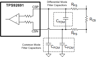
 Figure 20. Current Sense Amplifier Input Filter Options
An optional common-mode or differential mode low-pass filter implementation, as shown in Figure 20, can be used to smooth out the effects of large output current ripple and switching current spikes caused by diode reverse recovery. TI recommends a filter resistance in the range of 10 Ω to 100 Ω to limit the additional offset caused by amplifier bias current and achieve best accuracy and line regulation.
7.3.5 Transconductance Error Amplifier
The internal transconductance amplifier generates an error signal proportional to the difference between the LED current sense feedback voltage and the external IADJ input voltage. Closed-loop regulation is achieved by connecting a compensation network to the output of the error amplifier. In most LED driver applications, a stable response can be achieved by connecting a capacitor across the COMP output and ground to implement a simple integral compensator. TI recommends a capacitor value between 10 nF and 100 nF as a good starting point. Higher closed-loop bandwidth can be achieved by implementing a proportional-integral compensator consisting of a series resistor and a capacitor network connected across the COMP output and ground. Based on the converter topology, the compensation network should be tuned to achieve a minimum of 60° of phase margin and 10 dB of gain margin. The Application and Implementation section presents detailed equations.
7.3.6 Switch Current Sense and Internal Slope Compensation
The main MOSFET current is monitored by the IS input pin to implement peak current mode control. The GATE output duty cycle is derived by comparing the peak switch current, measured by the RIS resistor, to the internal COMP voltage threshold. An internal slope signal is added to the measured sense voltage, VIS, to prevent subharmonic oscillations for duty cycles greater than 50%. The linear slope voltage, VSL, of fixed amplitude 200 mV, is derived from a 100-µA sawtooth ramp current synchronized to the internal oscillator frequency. An internal blanking circuit prevents MOSFET switching current spike propagation and premature termination of duty cycle by internally shunting the IS input for 150 ns after the beginning of the new switching period. TI recommends an external low-pass RC filter with resistor values ranging from 100 Ω to 500 Ω for additional noise suppression when operating in the dropout region (VIN less than 7 V).
Cycle-by-cycle current limit is accomplished by a redundant internal comparator, which immediately terminates the GATE output when the IS input voltage, VIS, exceeds 525-mV (typ) threshold. Upon a current limit event, the SS and COMP pin are internally grounded to reset the state of the controller. The GATE output is enabled after the expiration of the 35-µs internal fault timer and a new start-up sequence is initiated through the SS pin.
7.3.7 Analog Adjust Input
The voltage across the LED current sense resistor, V(CSP–CSN), is regulated to the analog adjust input voltage, VIADJ, scaled by the current sense amplifier voltage gain of 14. The LED current can be linearly adjusted by varying the voltage on IADJ from 140 mV to 2.25 V using either a resistor divider from VCC or a voltage source. The IADJ pin can be connected to VCC through an external resistor to set LED current based on the 2.42-V internal reference voltage. Figure 21 shows different methods to set the IADJ voltage. The IADJ input can be used in conjunction with a NTC resistor to implement thermal foldback protection as shown in Figure 21(b). A PWM signal in conjunction with first- or second-order low-pass filter can be used to program the IADJ voltage as shown in Figure 21(c).

- Static reference setting resistor divider from VCC
- Thermal fold-back circuit using external NTC resistor
- Analog dimming achieved by low-pass filtering external PWM signal
7.3.8 PWM Input and Series Dimming FET Gate Driver Output
The TPS92691/-Q1 incorporates a dimming input (PWM) for pulse-width modulating the output LED current. The brightness of the LEDs can be linearly varied by modulating the duty cycle of the pulsating voltage source connected to the PWM input pin. Driving the PWM input below 2.3 V (typ) turns off switching, parks the oscillator, disconnects the COMP pin, and sets the DDRV output to GND in order to maintain the charge on the compensation network and output capacitors. On the rising edge of the PWM input voltage (VPWM > 2.5 V), the GATE and DDRV outputs are enabled to ramp the inductor current to the previous steady-state value. The COMP pin is connected and the error amplifier and oscillator are enabled only when the switch current sense voltage VIS exceeds the COMP voltage, VCOMP, thus immediately forcing the converter into steady-state operation with minimum LED current overshoot. The PWM pin should be connected to the VCC if dimming is not required. An internal pulldown resistor sets the input to logic-low and disables the part when the pin is disconnected or left floating.
 Figure 22. Series Dimming FET Connections
The DDRV output follows the PWM input signal and is capable of sinking and sourcing up to 500 mA of peak current to control a low-side series connected N-channel dimming FET. Alternatively, the DDRV output can be translated with an external level-shift circuit to drive a high-side series P-channel dimming FET as shown in Figure 22. The series dimming FET is required to achieve high contrast ratio as it ensures fast rise and fall times of the LED current in response to the PWM input. Without any dimming FET, the rise and fall times are limited by the inductor slew rate and the closed-loop bandwidth of the system. Leave the DDRV pin unconnected if not used.
7.3.9 Soft-Start
The soft-start feature helps the regulator gradually reach the steady-state operating point, thus reducing startup stresses and surges. The TPS92691/-Q1 clamps the COMP pin to the SS pin, separated by a diode, until LED current nears the regulation threshold. The internal 10-µA soft-start current source gradually increases the voltage on an external soft-start capacitor CSS connected to the SS pin. This results in a gradual rise of the COMP voltage from GND.
The internal 10-µA current source turns on when VCC exceeds the UVLO threshold. At the beginning of the soft-start sequence, the SS pulldown switch is active and is released when the voltage VSS drops below 25 mV. The SS pin can also be pulled down by an external switch to stop switching. When the SS pin is externally driven to enable switching, the slew-rate on the COMP pin should be controlled by choosing a compensation capacitor that avoids large startup transients. The value of CSS should be large enough to charge the output capacitor during the soft-start transition period.
7.3.10 Current Monitor Output
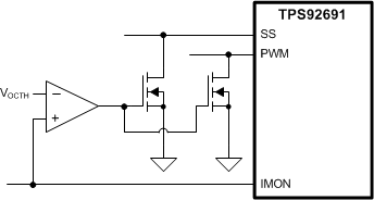
The IMON pin voltage represents the LED current measured by the rail-to-rail current sense amplifier across the external current shunt resistor. The linear relationship between the IMON voltage and LED current includes the amplifier gain-factor of 14 (see Figure 14). The IMON output can be connected to an external microcontroller or comparator to facilitate LED open, short, or cable harness fault detection and mitigation based on programmable threshold VOCTH. The IMON voltage is internally clamped to 3.7 V.
 Figure 23. LED Overcurrent Protection using IMON Output
7.3.11 Overvoltage Protection
The TPS92691/-Q1 device includes a dedicated OVP pin which can be used for either input or output overvoltage protection. This pin features a precision 1.24 V (typ) threshold with 20-µA (typ) of hysteresis current. The overvoltage threshold limit is set by a resistor divider network from the input or output terminal to GND. When the OVP pin voltage exceeds the reference threshold, the GATE and DDRV pins are immediately pulled low and the SS and COMP capacitors are discharged. The GATE is enabled and a new startup sequence is initiated after the voltage drops below the hysteresis threshold set by the 20-µA source current and the external resistor divider.
7.3.12 Thermal Protection
Internal thermal shutdown circuitry is implemented to protect the controller in the event the maximum junction temperature is exceeded. When activated, typically at 175°C, the controller is forced into a shutdown mode, disabling the internal regulator. This feature is designed to prevent overheating and damage to the device.
7.4 Device Functional Modes
This device has no additional functional modes.