ZHCSGY7B October   2017  – January 2018 TPS92830-Q1

PRODUCTION DATA.  

  1. 特性
  2. 应用
  3. 说明
    1.     简化原理图
  4. 修订历史记录
  5. 说明 (续)
  6. Pin Configuration and Functions
    1.     Pin Functions
  7. Specifications
    1. 7.1 Absolute Maximum Ratings
    2. 7.2 ESD Ratings
    3. 7.3 Recommended Operating Conditions
    4. 7.4 Thermal Information
    5. 7.5 Electrical Characteristics
    6. 7.6 Timing Requirements
    7. 7.7 Typical Characteristics
  8. Detailed Description
    1. 8.1 Overview
    2. 8.2 Functional Block Diagram
    3. 8.3 Feature Description
      1. 8.3.1 Device Bias
        1. 8.3.1.1 Power-On-Reset (POR)
        2. 8.3.1.2 Current Reference (IREF)
        3. 8.3.1.3 Low-Current Fault Mode
      2. 8.3.2 Charge Pump
        1. 8.3.2.1 Charge Pump Architecture
      3. 8.3.3 Constant-Current Driving
        1. 8.3.3.1 High-Side Current Sense
        2. 8.3.3.2 High-Side Current Driving
        3. 8.3.3.3 Gate Overdrive Voltage Protection
        4. 8.3.3.4 High-Precision Current Regulation
        5. 8.3.3.5 Parallel MOSFET Driving
      4. 8.3.4 PWM Dimming
        1. 8.3.4.1 Supply Dimming
        2. 8.3.4.2 PWM Dimming by Input
        3. 8.3.4.3 Internal Precision PWM Generator
        4. 8.3.4.4 Full Duty-Cycle Switch
      5. 8.3.5 Analog Dimming
        1. 8.3.5.1 Analog Dimming Topology
        2. 8.3.5.2 Internal High-Precision Pullup Current Source
      6. 8.3.6 Output Current Derating
        1. 8.3.6.1 Output-Current Derating Topology
      7. 8.3.7 Diagnostics and Fault
        1. 8.3.7.1 LED Short-to-GND Detection
        2. 8.3.7.2 LED Short-to-GND Auto Retry
        3. 8.3.7.3 LED Open-Circuit Detection
        4. 8.3.7.4 LED Open-Circuit Auto Retry
        5. 8.3.7.5 Dropout-Mode Diagnostics
        6. 8.3.7.6 Overtemperature Protection
        7. 8.3.7.7 FAULT Bus Output With One-Fails–All-Fail
        8. 8.3.7.8 Fault Table
    4. 8.4 Device Functional Modes
      1. 8.4.1 Undervoltage Lockout, V(IN) < V(UVLO)
      2. 8.4.2 Normal Operation (V(IN) ≥ 4.5 V, V(IN) > V(LED) + 0.5 V)
      3. 8.4.3 Low-Voltage Dropout
      4. 8.4.4 Fault Mode (Fault Is Detected)
  9. Application and Implementation
    1. 9.1 Application Information
    2. 9.2 Typical Applications
      1. 9.2.1 Typical Application for Automotive Exterior Lighting With One-Fails–All-Fail
        1. 9.2.1.1 Design Requirements
        2. 9.2.1.2 Detailed Design Procedure
        3. 9.2.1.3 Application Curves
      2. 9.2.2 High-Precision Dual-Brightness PWM Generation
        1. 9.2.2.1 Dual-Brightness Application
        2. 9.2.2.2 Design Requirements
        3. 9.2.2.3 Detailed Design Procedure
        4. 9.2.2.4 Application Curve
      3. 9.2.3 Driving High-Current LEDs With Parallel MOSFETs
        1. 9.2.3.1 Application Curves
  10. 10Layout
    1. 10.1 Layout Guidelines
    2. 10.2 Layout Example
  11. 11器件和文档支持
    1. 11.1 接收文档更新通知
    2. 11.2 社区资源
    3. 11.3 商标
    4. 11.4 静电放电警告
    5. 11.5 Glossary
  12. 12机械、封装和可订购信息

封装选项

机械数据 (封装 | 引脚)
散热焊盘机械数据 (封装 | 引脚)
订购信息

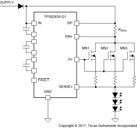
Parallel MOSFET Driving

The TPS92830-Q1 device is designed to support parallel N-channel MOSFETs driving within the same channel. To balance heat dissipation, multiple MOSFETs could be paralleled together. A ballast resistor for each MOSFET is recommended to balance current distribution among parallel MOSFETs.

Larger variation on threshold mismatches requires larger ballast resistors. V(TH_MISMATCH) is the threshold for mismatches within the same batch of MOSFETs. I(CH_MISMATCH) is the allowed mismatch current between the parallel channels. Typically, I(CH_MISMATCH) can be set to 10% of full-range current. The ballast resistor value is set as calculated in the following equation.

Equation 2. TPS92830-Q1 eq02-Rballast_SLIS178.gif

The ballast resistor typically ranges from hundreds of milliohms to several ohms depending on the channel current and MOSFET threshold-voltage variations.
TPS92830-Q1 MOSFET_Parallel_Driving_Support_SLIS178.gifFigure 22. Parallel MOSFET Driving