ZHCSLS0B July 2022 – April 2024 TPS929240-Q1
PRODUCTION DATA
- 1
- 1 特性
- 2 应用
- 3 说明
- 4 Pin Configuration and Functions
- 5 Specifications
-
6 Detailed Description
- 6.1 Overview
- 6.2 Functional Block Diagram
- 6.3
Feature Description
- 6.3.1 Device Bias and Power
- 6.3.2 Constant Current Output
- 6.3.3 PWM Dimming
- 6.3.4 FAIL-SAFE State Operation
- 6.3.5 On-Chip, 8-Bit, Analog-to-Digital Converter (ADC)
- 6.3.6
Diagnostic and Protection in NORMAL State
- 6.3.6.1 VBAT Undervoltage Lockout Diagnostics in NORMAL state
- 6.3.6.2 Low-Supply Warning Diagnostics in NORMAL State
- 6.3.6.3 Supply Undervoltage Diagnostics in NORMAL State
- 6.3.6.4 Reference Diagnostics in NORMAL state
- 6.3.6.5 Pre-Thermal Warning in NORMAL state
- 6.3.6.6 Overtemperature Protection in NORMAL state
- 6.3.6.7 Overtemperature Shutdown in NORMAL state
- 6.3.6.8 LED Open-Circuit Diagnostics in NORMAL state
- 6.3.6.9 LED Short-Circuit Diagnostics in NORMAL state
- 6.3.6.10 Single-LED Short-Circuit Detection in NORMAL state
- 6.3.6.11 EEPROM CRC Error in NORMAL state
- 6.3.6.12 Communication Loss Diagnostic in NORMAL State
- 6.3.6.13 Fault Masking in NORMAL state
- 53
- 6.3.7
Diagnostic and Protection in FAIL-SAFE states
- 6.3.7.1 Supply Undervoltage Lockout Diagnostics in FAIL-SAFE states
- 6.3.7.2 Low-Supply Warning Diagnostics in FAIL-SAFE states
- 6.3.7.3 Supply Undervoltage Diagnostics in FAIL-SAFE State
- 6.3.7.4 Reference Diagnostics in FAIL-SAFE states
- 6.3.7.5 Pre-Thermal Warning in FAIL-SAFE state
- 6.3.7.6 Overtemperature Protection in FAIL-SAFE state
- 6.3.7.7 Overtemperature Shutdown in FAIL-SAFE state
- 6.3.7.8 LED Open-Circuit Diagnostics in FAIL-SAFE state
- 6.3.7.9 LED Short-Circuit Diagnostics in FAIL-SAFE state
- 6.3.7.10 Single-LED Short-Circuit Detection in FAIL-SAFE state
- 6.3.7.11 EEPROM CRC Error in FAIL-SAFE State
- 6.3.7.12 Fault Masking in FAIL-SAFE state
- Diagnostics Table in FAIL-SAFE State
- 6.3.8 OFAF Setup In FAIL-SAFE state
- 6.3.9 ERR Output
- 6.4 Device Functional Modes
- 6.5 Programming
- 6.6 Register Maps
- 7 Application and Implementation
- 8 Device and Documentation Support
- 9 Revision History
- 10Mechanical, Packaging, and Orderable Information
封装选项
请参考 PDF 数据表获取器件具体的封装图。
机械数据 (封装 | 引脚)
- DCP|38
散热焊盘机械数据 (封装 | 引脚)
- DCP|38
订购信息
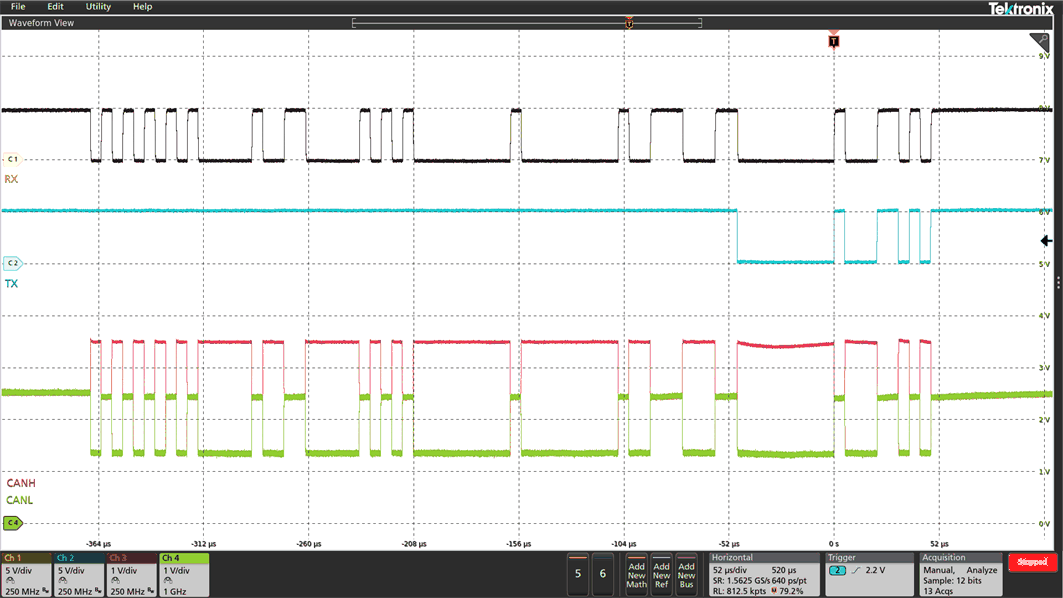
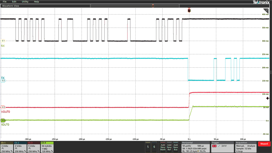
7.2.4 Application Curves

| CH1 = RX | CH2 = TC | CH3 = CANH |
| CH4 = CANL |

| CH1 = RX | CH2 = TX | CH3 = V(OUT0) |
| CH4 = I(OUT0) |