ZHCSIF5G December 2015 – July 2024 TPS99000-Q1
PRODUCTION DATA
- 1
- 1 特性
- 2 应用
- 3 说明
- 4 Pin Configuration and Functions
-
5 Specifications
- 5.1 Absolute Maximum Ratings
- 5.2 ESD Ratings
- 5.3 Recommended Operating Conditions
- 5.4 Thermal Information
- 5.5 Electrical Characteristics—Transimpedance Amplifier Parameters
- 5.6 Electrical Characteristics—Digital to Analog Converters
- 5.7 Electrical Characteristics—Analog to Digital Converter
- 5.8 Electrical Characteristics—FET Gate Drivers
- 5.9 Electrical Characteristics—Photo Comparator
- 5.10 Electrical Characteristics—Voltage Regulators
- 5.11 Electrical Characteristics—Temperature and Voltage Monitors
- 5.12 Electrical Characteristics—Current Consumption
- 5.13 Power-Up Timing Requirements
- 5.14 Power-Down Timing Requirements
- 5.15 Timing Requirements—Sequencer Clock
- 5.16 Timing Requirements—Host and Diagnostic Port SPI Interface
- 5.17 Timing Requirements—ADC Interface
- 5.18 Switching Characteristics
-
6 Detailed Description
- 6.1 Overview
- 6.2 Functional Block Diagram
- 6.3
Feature Description
- 6.3.1
Illumination Control
- 6.3.1.1 Illumination System High Dynamic Range Dimming Overview
- 6.3.1.2 Illumination Control Loop
- 6.3.1.3 Continuous Mode Operation
- 6.3.1.4
Discontinuous Mode Operation
- 6.3.1.4.1 Discontinuous Mode Pulse Width Limit
- 6.3.1.4.2 COMPOUT_LOW Timer in Discontinuous Operation
- 6.3.1.4.3 Dimming Within Discontinuous Operation Range
- 6.3.1.4.4 Multiple Pulse Heights to Increase Bit Depth
- 6.3.1.4.5 TIA Gain Adjustment
- 6.3.1.4.6 Current Limit in Discontinuous Mode
- 6.3.1.4.7 CMODE Big Cap Mode in Discontinuous Operation
- 6.3.2 Over-Brightness Detection
- 6.3.3 Analog to Digital Converter
- 6.3.4 Power Sequencing and Monitoring
- 6.3.5 DMD Mirror Voltage Regulator
- 6.3.6 Low Dropout Regulators
- 6.3.7 System Monitoring Features
- 6.3.8 Communication Ports
- 6.3.1
Illumination Control
- 6.4 Device Functional Modes
- 6.5 Register Maps
- 7 Application and Implementation
- 8 Power Supply Recommendations
- 9 Layout
- 10Device and Documentation Support
- 11Revision History
- 12Mechanical, Packaging, and Orderable Information
封装选项
机械数据 (封装 | 引脚)
- PZP|100
散热焊盘机械数据 (封装 | 引脚)
- PZP|100
订购信息
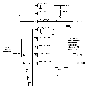
6.3.5 DMD Mirror Voltage Regulator
The DMD mirror voltage regulator generates three high-voltage supply rails: DMD_VRESET, DMD_VBIAS, and DMD_VOFFSET. The DMD regulator uses a switching regulator where the inductor is time-shared between all three supplies. The inductor is charged up to a certain current level and then discharged into one of the three supplies. In cases where a supply does not need additional charge, the time slot normally allocated to that supply is skipped and the supplies requiring more charge receive all of the charging time.
For proper operation, specific bulk capacitance values are required for each supply rail. Refer to Electrical Characteristics—Temperature and Voltage Monitors for recommended values for the capacitors. The regulator contains active power down/discharge circuits. To meet timing requirements, total capacitance (actual capacitance, not the nominal) must not exceed these levels by substantial amounts, as defined in Electrical Characteristics—Temperature and Voltage Monitors. Power-down timing should be verified in each specific system design. Too low of a total capacitance will result in excessive ripple on the supply rails which may impact DMD mirror dynamic behavior. Care should be taken to use capacitors that maintain the recommended minimum capacitance over the expected operating device temperature range. Large-size packages are required here that do not lose so much capacitance at high voltages.
Although the average current drawn by the DMD on these supplies is small (10s of mA worst case), the peak currents can be several amps over 10s of nano-seconds. To supply this peak current, the use of small-value, high-frequency decoupling capacitors should be included as close as practical to the DMD power input pins.
 Figure 6-31 DMD Voltage Regulator Circuit