ZHCSIF5G December 2015 – July 2024 TPS99000-Q1
PRODUCTION DATA
- 1
- 1 特性
- 2 应用
- 3 说明
- 4 Pin Configuration and Functions
-
5 Specifications
- 5.1 Absolute Maximum Ratings
- 5.2 ESD Ratings
- 5.3 Recommended Operating Conditions
- 5.4 Thermal Information
- 5.5 Electrical Characteristics—Transimpedance Amplifier Parameters
- 5.6 Electrical Characteristics—Digital to Analog Converters
- 5.7 Electrical Characteristics—Analog to Digital Converter
- 5.8 Electrical Characteristics—FET Gate Drivers
- 5.9 Electrical Characteristics—Photo Comparator
- 5.10 Electrical Characteristics—Voltage Regulators
- 5.11 Electrical Characteristics—Temperature and Voltage Monitors
- 5.12 Electrical Characteristics—Current Consumption
- 5.13 Power-Up Timing Requirements
- 5.14 Power-Down Timing Requirements
- 5.15 Timing Requirements—Sequencer Clock
- 5.16 Timing Requirements—Host and Diagnostic Port SPI Interface
- 5.17 Timing Requirements—ADC Interface
- 5.18 Switching Characteristics
-
6 Detailed Description
- 6.1 Overview
- 6.2 Functional Block Diagram
- 6.3
Feature Description
- 6.3.1
Illumination Control
- 6.3.1.1 Illumination System High Dynamic Range Dimming Overview
- 6.3.1.2 Illumination Control Loop
- 6.3.1.3 Continuous Mode Operation
- 6.3.1.4
Discontinuous Mode Operation
- 6.3.1.4.1 Discontinuous Mode Pulse Width Limit
- 6.3.1.4.2 COMPOUT_LOW Timer in Discontinuous Operation
- 6.3.1.4.3 Dimming Within Discontinuous Operation Range
- 6.3.1.4.4 Multiple Pulse Heights to Increase Bit Depth
- 6.3.1.4.5 TIA Gain Adjustment
- 6.3.1.4.6 Current Limit in Discontinuous Mode
- 6.3.1.4.7 CMODE Big Cap Mode in Discontinuous Operation
- 6.3.2 Over-Brightness Detection
- 6.3.3 Analog to Digital Converter
- 6.3.4 Power Sequencing and Monitoring
- 6.3.5 DMD Mirror Voltage Regulator
- 6.3.6 Low Dropout Regulators
- 6.3.7 System Monitoring Features
- 6.3.8 Communication Ports
- 6.3.1
Illumination Control
- 6.4 Device Functional Modes
- 6.5 Register Maps
- 7 Application and Implementation
- 8 Power Supply Recommendations
- 9 Layout
- 10Device and Documentation Support
- 11Revision History
- 12Mechanical, Packaging, and Orderable Information
封装选项
机械数据 (封装 | 引脚)
- PZP|100
散热焊盘机械数据 (封装 | 引脚)
- PZP|100
订购信息
7.2.1.2.1 Photodiode Considerations
Placement of the photodiode within the optical path is critical to system performance. Carefully optimizing the placement and electrical response of the photodiode will yield the widest dynamic range for dimming. Treatment of photodiode considerations are addressed in the Photodiode Selection and Placement Guide (DLPA082).
Several factors for the photodiode should be considered:
- Position:
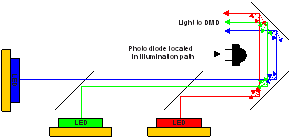
- Ideally, a position in the illumination path (Figure 7-2) should be located that produces strong, but also balanced amplitude signal responses from each of the three LEDs at the system's target white point. Imbalance between the three channels due to non-ideal placement of the detector will limit dynamic range of the dimming system. The TIA supports an RGB trim function to help re-balance an imbalanced system. This feature is useful for completing the process of optimizing the balance of the amplitude signal responses from each LED. But it is still advisable to take care in the design of the illumination path such that the natural balance of the colors is as ideal as practical.
- An additional consideration when determining position of photodiode is back scattered light from the projection path. Some amount of on state light will reflect backwards from the surfaces of the projection lens and other objects in the light path after the DMD. If the photodiode is placed in a position that is illuminated by this back scattered light, the photodiode will see a mixture of true illumination light plus this back scattered output light. If the back scattered light is significant, the illumination control loop will be impacted. Also, the back scatter is dependent on the video content (that is, a solid white pattern may cause more back scatter than a solid black pattern), which impacts the full-on full-off contrast.
- Irradiance on the Photodiode:
- It is also important that the irradiance on the photodiode is not too high or too low. A high magnitude of irradiance can cause saturation and slower response from the photodiode. This varies depending on the specific photodiode selected for use. The TPS99000-Q1 provides a negative LDO and negative voltage source to provide a low noise –8V reference for reverse biasing the photodiode. Reverse biasing the photodiode (photo conductive mode) increases the amount of irradiance the photodiode can accept without saturating as compared to a zero bias case (photovoltaic mode). On the other hand, a low magnitude of irradiance can make the system more susceptible to noise, including photodiode dark current. It is best to operate at photodiode current levels high enough so that dark current is negligible to avoid potential issues due to other noise sources (noise on cabling, grounding, and so on).
- Cable to remote PD placement:
- If the photodiode is located remotely it is recommended to use a low capacitance cable and minimize the cable length. At a minimum: for noise rejection, use a one conductor shielded cable with the photodiode bias (cathode) connected to the cable shield and the photodiode output (anode) connected to the inner conductor. Better noise rejection is possible using shielded two conductor cables with the shield tied to a low noise ground. Experiments may be necessary to determine an optimal photodiode position to achieve adequate response balance between the colors and an acceptable irradiance level. Care must be taken to not exceed the maximum total photodiode capacitance (diode plus cable and connectors) as specified in Section 5.5. TIA design includes adjustable feedback capacitance to optimize response for specific solutions. DLPC23x-Q1 flash configuration options allow tuning of this feedback capacitance for optimal slew rate and stability performance.
 Figure 7-2 Photodiode Placement
The photodiode conditioning circuits include several features to improve performance and integration:
- Independent red, green, and blue parameters for gain and offset
- Selectable feedback capacitance
- Integrated negative LDO, to provide photodiode reverse bias