ZHCSIF5G December 2015 – July 2024 TPS99000-Q1
PRODUCTION DATA
- 1
- 1 特性
- 2 应用
- 3 说明
- 4 Pin Configuration and Functions
-
5 Specifications
- 5.1 Absolute Maximum Ratings
- 5.2 ESD Ratings
- 5.3 Recommended Operating Conditions
- 5.4 Thermal Information
- 5.5 Electrical Characteristics—Transimpedance Amplifier Parameters
- 5.6 Electrical Characteristics—Digital to Analog Converters
- 5.7 Electrical Characteristics—Analog to Digital Converter
- 5.8 Electrical Characteristics—FET Gate Drivers
- 5.9 Electrical Characteristics—Photo Comparator
- 5.10 Electrical Characteristics—Voltage Regulators
- 5.11 Electrical Characteristics—Temperature and Voltage Monitors
- 5.12 Electrical Characteristics—Current Consumption
- 5.13 Power-Up Timing Requirements
- 5.14 Power-Down Timing Requirements
- 5.15 Timing Requirements—Sequencer Clock
- 5.16 Timing Requirements—Host and Diagnostic Port SPI Interface
- 5.17 Timing Requirements—ADC Interface
- 5.18 Switching Characteristics
-
6 Detailed Description
- 6.1 Overview
- 6.2 Functional Block Diagram
- 6.3
Feature Description
- 6.3.1
Illumination Control
- 6.3.1.1 Illumination System High Dynamic Range Dimming Overview
- 6.3.1.2 Illumination Control Loop
- 6.3.1.3 Continuous Mode Operation
- 6.3.1.4
Discontinuous Mode Operation
- 6.3.1.4.1 Discontinuous Mode Pulse Width Limit
- 6.3.1.4.2 COMPOUT_LOW Timer in Discontinuous Operation
- 6.3.1.4.3 Dimming Within Discontinuous Operation Range
- 6.3.1.4.4 Multiple Pulse Heights to Increase Bit Depth
- 6.3.1.4.5 TIA Gain Adjustment
- 6.3.1.4.6 Current Limit in Discontinuous Mode
- 6.3.1.4.7 CMODE Big Cap Mode in Discontinuous Operation
- 6.3.2 Over-Brightness Detection
- 6.3.3 Analog to Digital Converter
- 6.3.4 Power Sequencing and Monitoring
- 6.3.5 DMD Mirror Voltage Regulator
- 6.3.6 Low Dropout Regulators
- 6.3.7 System Monitoring Features
- 6.3.8 Communication Ports
- 6.3.1
Illumination Control
- 6.4 Device Functional Modes
- 6.5 Register Maps
- 7 Application and Implementation
- 8 Power Supply Recommendations
- 9 Layout
- 10Device and Documentation Support
- 11Revision History
- 12Mechanical, Packaging, and Orderable Information
封装选项
机械数据 (封装 | 引脚)
- PZP|100
散热焊盘机械数据 (封装 | 引脚)
- PZP|100
订购信息
6.3.1.3.2 Continuous Mode Driver Distortion and Blanking Current
 Figure 6-7 First
Generation/Legacy System Pulse Distortion Example
Figure 6-7 First
Generation/Legacy System Pulse Distortion ExampleAs seen in Figure 6-7, the actual LED current pulse is distorted due to the rising (Tr) and falling (Tf) edges rates not being equal, and/or the turn-on (Tp1) and turn-off (Tp2) propagation delays not being equal. The rising edge turn-on time of the current pulse is primarily a function of the voltage across the inductor and the desired current, plus the inductor current initial condition. This distortion causes both the time attenuation and amplitude attenuation of the pulse to become non-linear functions of the control settings. This can lead to image artifacts.
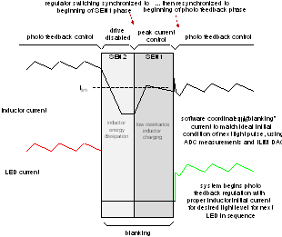
Blanking time is the period of no light output in between two LED segments. The inductor current during this time is called blanking current. This current is controlled to provide an optimized Tr and Tf.
Blanking current control reduces image artifacts by preventing light overshoot and undershoot.
The blanking current time periods are split into two parts. The first is a dissipation phase where the residual current in the inductor from the previous light pulse is reduced using a dissipative shunt. The second phase is a non-dissipative (low series resistance) shunt phase, where the inductor is charged up to the appropriate current for the next light pulse before current is applied to the LED. This process is illustrated in Figure 6-8.
 Figure 6-8 Blanking
Current Discharge/Charge Cycles
Figure 6-8 Blanking
Current Discharge/Charge CyclesDuring the first phase of the blanking time, shunt 2 (S_EN2) is enabled while the LEDs are disconnected. This places a load with a higher effective resistance in place of the LEDs. The residual energy in the inductor is dissipated into this load and the inductor current decreases rapidly. Without this feature, a high current in one pulse could cause excessive brightness in the next pulse.
During the second phase of the blanking time, the LED driver charges the inductor through a short circuit shunt (S_EN1). Charging continues until the peak current limit is reached. The peak current limit is set by the ILIM DAC. The peak current limit setting is coordinated by DLPC23x-Q1 software to match the expected operating current during photo feedback operation. (The expected current level is determined from ADC measurements of LED current during prior frames.) When the blanking current time period is over, the S_EN1 short circuit shunt is turned off, the next LED is enabled, the DRV_EN signal is toggled, and the system reverts to photo feedback, hysteretic operation. Because the inductor is precharged to the ideal current and the system capacitance is low, light output rising edge is extremely fast, and the transition to stable hysteretic control is nearly immediate. This results in a more rectangular pulse. An illustration of the current paths is shown in Figure 6-9.
 Figure 6-9 Blanking
Current Paths
Figure 6-9 Blanking
Current PathsPrecise control of the LED pulse shape results in greater dimming range, more display bit depth, and better color and gray ramp accuracy.