ZHCSIF5G December 2015 – July 2024 TPS99000-Q1
PRODUCTION DATA
- 1
- 1 特性
- 2 应用
- 3 说明
- 4 Pin Configuration and Functions
-
5 Specifications
- 5.1 Absolute Maximum Ratings
- 5.2 ESD Ratings
- 5.3 Recommended Operating Conditions
- 5.4 Thermal Information
- 5.5 Electrical Characteristics—Transimpedance Amplifier Parameters
- 5.6 Electrical Characteristics—Digital to Analog Converters
- 5.7 Electrical Characteristics—Analog to Digital Converter
- 5.8 Electrical Characteristics—FET Gate Drivers
- 5.9 Electrical Characteristics—Photo Comparator
- 5.10 Electrical Characteristics—Voltage Regulators
- 5.11 Electrical Characteristics—Temperature and Voltage Monitors
- 5.12 Electrical Characteristics—Current Consumption
- 5.13 Power-Up Timing Requirements
- 5.14 Power-Down Timing Requirements
- 5.15 Timing Requirements—Sequencer Clock
- 5.16 Timing Requirements—Host and Diagnostic Port SPI Interface
- 5.17 Timing Requirements—ADC Interface
- 5.18 Switching Characteristics
-
6 Detailed Description
- 6.1 Overview
- 6.2 Functional Block Diagram
- 6.3
Feature Description
- 6.3.1
Illumination Control
- 6.3.1.1 Illumination System High Dynamic Range Dimming Overview
- 6.3.1.2 Illumination Control Loop
- 6.3.1.3 Continuous Mode Operation
- 6.3.1.4
Discontinuous Mode Operation
- 6.3.1.4.1 Discontinuous Mode Pulse Width Limit
- 6.3.1.4.2 COMPOUT_LOW Timer in Discontinuous Operation
- 6.3.1.4.3 Dimming Within Discontinuous Operation Range
- 6.3.1.4.4 Multiple Pulse Heights to Increase Bit Depth
- 6.3.1.4.5 TIA Gain Adjustment
- 6.3.1.4.6 Current Limit in Discontinuous Mode
- 6.3.1.4.7 CMODE Big Cap Mode in Discontinuous Operation
- 6.3.2 Over-Brightness Detection
- 6.3.3 Analog to Digital Converter
- 6.3.4 Power Sequencing and Monitoring
- 6.3.5 DMD Mirror Voltage Regulator
- 6.3.6 Low Dropout Regulators
- 6.3.7 System Monitoring Features
- 6.3.8 Communication Ports
- 6.3.1
Illumination Control
- 6.4 Device Functional Modes
- 6.5 Register Maps
- 7 Application and Implementation
- 8 Power Supply Recommendations
- 9 Layout
- 10Device and Documentation Support
- 11Revision History
- 12Mechanical, Packaging, and Orderable Information
封装选项
机械数据 (封装 | 引脚)
- PZP|100
散热焊盘机械数据 (封装 | 引脚)
- PZP|100
订购信息
6.3.4.1 Power Monitoring
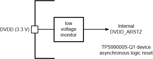
Main asynchronous digital logic reset (DVDD_RSTZ) – Monitor of the main power of the 3.3V power supply input to the TPS99000-Q1. This monitor output is used as an asynchronous reset for all of the digital logic inside TPS99000-Q1.
 Figure 6-28 Internal DVDD Monitor
The PROJ_ON pin is the main on/off switch for the DLP subsystem. 1 is ON, 0 is OFF. Once DVDD_ARSTZ is released, TPS99000-Q1 will begin sampling the PROJ_ON pin. If it is low, the system stays in the OFF state. If it goes high, TPS99000-Q1 begins to progress through the power-on process.
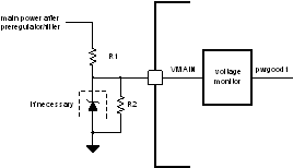
The TPS99000-Q1 includes a VMAIN brown out monitor function. A voltage monitor observes the voltage on the VMAIN input pin, as shown in Figure 6-29. The Zener may be necessary for overvoltage protection of the pin, in case the voltage being monitored has the potential to go high, such as a battery input.
Either PROJ_ON or VMAIN may be used to turn the system on and off, and doing so will remove power to the DLPC23x-Q1. For fast control of turning the display on and off without removing power to the DLPC23x-Q1, change the operating mode of the DLPC23x-Q1 embedded software between 'Standby' and 'Display'.
 Figure 6-29 VMAIN Brown Out Monitor
This monitor is used to provide the DLP subsystem with an early warning that power to the unit is going away. The system will park the DMD mirrors and proceed to a ready-for-power-off state if the VMAIN input voltage falls below a fixed threshold. External resistors should be used to divide the input power rail. Once a VMAIN brownout occurs, the main power rails to the TPS99000-Q1 must remain within their operating ranges until the TPS99000-Q1 power-down is complete.
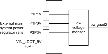
The main power rails to the chipset (6V, 3.3V, 1.8V, and 1.1V) are monitored with real-time power monitors as well. Each of these monitors is logically 'OR'ed together to produce the pwrgood2 signal in Figure 6-30.
 Figure 6-30 Real-Time Power Rail Monitors
Additionally, all power within the TPS99000-Q1 can be monitored by the ADC function. DLPC23x-Q1 software configures the ADC block to collect all voltage information in the system each frame. Any gross out of specification issues are captured and reported as system errors in the DLPC23x-Q1 system status.