ZHCSIF5G December 2015 – July 2024 TPS99000-Q1
PRODUCTION DATA
- 1
- 1 特性
- 2 应用
- 3 说明
- 4 Pin Configuration and Functions
-
5 Specifications
- 5.1 Absolute Maximum Ratings
- 5.2 ESD Ratings
- 5.3 Recommended Operating Conditions
- 5.4 Thermal Information
- 5.5 Electrical Characteristics—Transimpedance Amplifier Parameters
- 5.6 Electrical Characteristics—Digital to Analog Converters
- 5.7 Electrical Characteristics—Analog to Digital Converter
- 5.8 Electrical Characteristics—FET Gate Drivers
- 5.9 Electrical Characteristics—Photo Comparator
- 5.10 Electrical Characteristics—Voltage Regulators
- 5.11 Electrical Characteristics—Temperature and Voltage Monitors
- 5.12 Electrical Characteristics—Current Consumption
- 5.13 Power-Up Timing Requirements
- 5.14 Power-Down Timing Requirements
- 5.15 Timing Requirements—Sequencer Clock
- 5.16 Timing Requirements—Host and Diagnostic Port SPI Interface
- 5.17 Timing Requirements—ADC Interface
- 5.18 Switching Characteristics
-
6 Detailed Description
- 6.1 Overview
- 6.2 Functional Block Diagram
- 6.3
Feature Description
- 6.3.1
Illumination Control
- 6.3.1.1 Illumination System High Dynamic Range Dimming Overview
- 6.3.1.2 Illumination Control Loop
- 6.3.1.3 Continuous Mode Operation
- 6.3.1.4
Discontinuous Mode Operation
- 6.3.1.4.1 Discontinuous Mode Pulse Width Limit
- 6.3.1.4.2 COMPOUT_LOW Timer in Discontinuous Operation
- 6.3.1.4.3 Dimming Within Discontinuous Operation Range
- 6.3.1.4.4 Multiple Pulse Heights to Increase Bit Depth
- 6.3.1.4.5 TIA Gain Adjustment
- 6.3.1.4.6 Current Limit in Discontinuous Mode
- 6.3.1.4.7 CMODE Big Cap Mode in Discontinuous Operation
- 6.3.2 Over-Brightness Detection
- 6.3.3 Analog to Digital Converter
- 6.3.4 Power Sequencing and Monitoring
- 6.3.5 DMD Mirror Voltage Regulator
- 6.3.6 Low Dropout Regulators
- 6.3.7 System Monitoring Features
- 6.3.8 Communication Ports
- 6.3.1
Illumination Control
- 6.4 Device Functional Modes
- 6.5 Register Maps
- 7 Application and Implementation
- 8 Power Supply Recommendations
- 9 Layout
- 10Device and Documentation Support
- 11Revision History
- 12Mechanical, Packaging, and Orderable Information
封装选项
机械数据 (封装 | 引脚)
- PZP|100
散热焊盘机械数据 (封装 | 引脚)
- PZP|100
订购信息
6.3.1 Illumination Control
The illumination control function includes all blocks required to generate light for the DLP subsystem. The system is designed to support automotive applications requiring precise control of color and brightness over a wide dimming range. The complete dimming solution consists of hardware features included in both the DLPC23x-Q1 and TPS99000-Q1 along with DMD sequence data stored in the DLPC23x-Q1. These elements work together to provide a usable system dimming range of over 5000:1, with up to 8 bits per color supported.
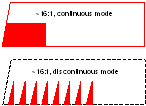
The illumination control function operates in two distinct modes to cover the full dimming range. These modes are referred to as continuous mode (CM) and discontinuous mode (DM).
 Figure 6-1 Comparison of Continuous and Discontinuous Mode Operation
Continuous mode features:
- High- to mid-brightness levels
- Rectangular light pulses created for each color
- Pulse amplitude and pulse width varied to adjust brightness level
Discontinuous mode features:
- Mid- to low-brightness levels
- A series of small triangular light pulses created for each color
- Number of pulses, pulse height, and LED current varied to adjust brightness level
The illumination control loop regulates the current supplied to the LEDs through a real-time photo feedback control loop. A broadband photodiode is placed in the illumination path of the DLP subsystem in a location that receives light from all three red/green/blue LEDs. For continuous mode operation, photo feedback is used to create a real-time hysteretic control loop to set the brightness levels for each LED. In discontinuous mode, photo feedback is used to set a peak brightness threshold for each light pulse.
To support illumination control, the TPS99000-Q1 includes numerous high-performance analog and mixed-signal blocks. These blocks include:
- A high-performance, ultra-wide dynamic range transimpedance amplifier (TIA) to convert photodiode current to a voltage, representing real-time LED brightness
- A high-speed comparator for photo feedback control
- A 12-bit DAC for photo feedback reference
- A 10-bit DAC for peak current limit adjustment
- Sync and drive enable outputs for synchronizing an external high-side PFET buck controller (LM3409)
- External FET drivers and control logic for selection of LEDs (FETs are external, but the drivers are internal)
- Two current shunt (by-pass) path FET controls, used to preregulate inductor current while light is disabled between colors, and to enable discontinuous mode operation
- A multi-purpose 12-bit ADC block with a dedicated two wire Kelvin input channel specifically for measuring LED current
- Hardware sample timer block that works in conjunction with DLPC23x-Q1 to provide configurable hardware timed samples of LED current and voltage, temperature, and so on.
- RGB specific multiplexed settings for most parameters, enabling independent control parameter optimization per color