ZHCSN32B June 2019 – July 2024 TPS99001-Q1
PRODUCTION DATA
- 1
- 1 特性
- 2 应用
- 3 说明
- 4 Pin Configuration and Functions
-
5 Specifications
- 5.1 Absolute Maximum Ratings
- 5.2 ESD Ratings
- 5.3 Recommended Operating Conditions
- 5.4 Thermal Information
- 5.5 Electrical Characteristics—Analog to Digital Converter
- 5.6 Electrical Characteristics—Voltage Regulators
- 5.7 Electrical Characteristics—Temperature and Voltage Monitors
- 5.8 Electrical Characteristics—Current Consumption
- 5.9 Power-Up Timing Requirements
- 5.10 Power-Down Timing Requirements
- 5.11 Timing Requirements—Sequencer Clock
- 5.12 Timing Requirements—Host and Diagnostic Port SPI Interface
- 5.13 Timing Requirements—ADC Interface
- 5.14 Switching Characteristics
-
6 Detailed Description
- 6.1 Overview
- 6.2 Functional Block Diagram
- 6.3 Feature Description
- 6.4 Device Functional Modes
- 6.5 Register Maps
- 7 Application and Implementation
- 8 Power Supply Recommendations
- 9 Layout
- 10Device and Documentation Support
- 11Revision History
- 12Mechanical, Packaging, and Orderable Information
5.10 Power-Down Timing Requirements
See (1)
| MIN | MAX | UNIT | |||
|---|---|---|---|---|---|
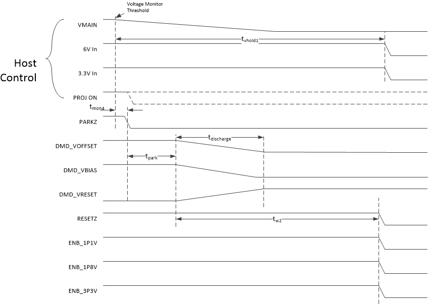
| tvhold1 | Host voltage hold time after VMAIN minimum
threshold reached. tmon4(max) + tpark(max) + tw2(max) |
VMAIN threshold to 6V and 3.3V power loss(2)(3) | 900 | μs | |
| tvhold2 | Host voltage hold time after PROJ_ON
deasserted. tmon5(max) + tpark(max) + tw2(max) |
VMAIN threshold to 6V and 3.3V power loss.(2)(3) | 1.78 | ms | |
| tmon4 | VMAIN monitoring time | Minimum voltage trip threshold to PARKZ falling edge | 52 | 120 | μs |
| tmon5 | PROJ_ON deassertion reaction time | Falling edge of PROJ_ON to PARKZ falling edge | 1 | ms | |
| tpark | DMD Park time | PARKZ falling edge to start DMD_VOFFSET discharge | 280 | μs | |
| tdischarge(4) | DMD voltage rail discharge time | VOFFSET Cout = 1μF VRESET Cout = 1μF VBIAS Cout = 0.47μF |
260 | μs | |
| tw2 | DMD voltage disables to RESETZ deassertion | Start of DMD voltage rail discharge to RESETZ falling edge | 500 | μs | |
(1) There are two methods for initiating the power-down sequence:
- VMAIN voltage decreases below its minimum threshold. This is typical if the TPS99001-Q1 is expected to initiate the power-down sequence when the main power is removed from the system. Note that the 6V and 3.3V input rails must remain within the operating range for a specified period of time after the power-down sequence begins.
- PROJ_ON low. This allows a host controller to initiate power down through a digital input to the TPS99001-Q1.
(2) 6V input rails include DRVR_PWR, VIN_DRST, VIN_LDOT_5V,
VIN_LDOA_3P3V, VIN_LDOT3P3V.
(3) 3.3V input rails include VDD_IO, DVDD, AVDD.
(4) The DMD specifies a maximum absolute voltage difference between
VBIAS and VOFFSET. To remain below this maximum voltage difference, VBIAS must
discharge faster than VOFFSET. This is accomplished by using a smaller
Cout capacitance for VBIAS to allow it to discharge quicker than
VOFFSET.
 Figure 5-2 Power
Down Timing—VMAIN Trigger
 Figure 5-3 Power
Down Timing—PROJ_ON Trigger