ZHCSN32B June 2019 – July 2024 TPS99001-Q1
PRODUCTION DATA
- 1
- 1 特性
- 2 应用
- 3 说明
- 4 Pin Configuration and Functions
-
5 Specifications
- 5.1 Absolute Maximum Ratings
- 5.2 ESD Ratings
- 5.3 Recommended Operating Conditions
- 5.4 Thermal Information
- 5.5 Electrical Characteristics—Analog to Digital Converter
- 5.6 Electrical Characteristics—Voltage Regulators
- 5.7 Electrical Characteristics—Temperature and Voltage Monitors
- 5.8 Electrical Characteristics—Current Consumption
- 5.9 Power-Up Timing Requirements
- 5.10 Power-Down Timing Requirements
- 5.11 Timing Requirements—Sequencer Clock
- 5.12 Timing Requirements—Host and Diagnostic Port SPI Interface
- 5.13 Timing Requirements—ADC Interface
- 5.14 Switching Characteristics
-
6 Detailed Description
- 6.1 Overview
- 6.2 Functional Block Diagram
- 6.3 Feature Description
- 6.4 Device Functional Modes
- 6.5 Register Maps
- 7 Application and Implementation
- 8 Power Supply Recommendations
- 9 Layout
- 10Device and Documentation Support
- 11Revision History
- 12Mechanical, Packaging, and Orderable Information
6.3.5.1 Windowed Watchdog Circuits
The TPS99001-Q1 contains two windowed watchdog circuits that can be used to detect malfunctions within the DLPC23x-Q1.
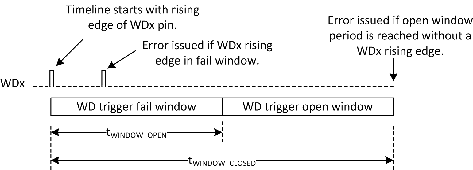
 Figure 6-6 Windowed Watchdog Function
The DLPC23x-Q1 software uses both watchdog circuits. Watchdog #1 (WD1) monitors the internal microprocessor of the DLPC23x-Q1 through a wire connection to a dedicated GPIO line from DLPC23x-Q1. Watchdog #2 (WD2) is used to monitor the DLPC23x-Q1 sequencer operation (through monitoring of the SEQ_STRT pin, wired to WD2 input).
When this function is enabled, two registers control the timing of the opening and closing of a watchdog trigger window. Process is initiated by a rising edge on the respective WDx pin. If another rising edge occurs before the WD trigger window opens, a watchdog error is issued. If the end of the open window period is reached without receiving a rising edge on WDx, an error is issued. The process restarts any time a WDx rising edge is received. The two watchdogs are independent.