ZHCSKO0B December 2019 – September 2021 TPSM53602
PRODUCTION DATA
- 1 特性
- 2 应用
- 3 说明
- 4 Revision History
- 5 Pin Configuration and Functions
- 6 Specifications
-
7 Detailed Description
- 7.1 Overview
- 7.2 Functional Block Diagram
- 7.3
Feature Description
- 7.3.1 Adjusting the Output Voltage
- 7.3.2 Switching Frequency
- 7.3.3 Input Capacitors
- 7.3.4 Output Capacitors
- 7.3.5 Output On/Off Enable (EN)
- 7.3.6 Programmable Undervoltage Lockout (UVLO)
- 7.3.7 Power Good (PGOOD)
- 7.3.8 Light Load Operation
- 7.3.9 Voltage Dropout
- 7.3.10 Overcurrent Protection (OCP)
- 7.3.11 Thermal Shutdown
- 7.4 Device Functional Modes
- 8 Application and Implementation
- 9 Power Supply Recommendations
- 10Layout
- 11Device and Documentation Support
- 12Mechanical, Packaging, and Orderable Information
7.3.5 Output On/Off Enable (EN)
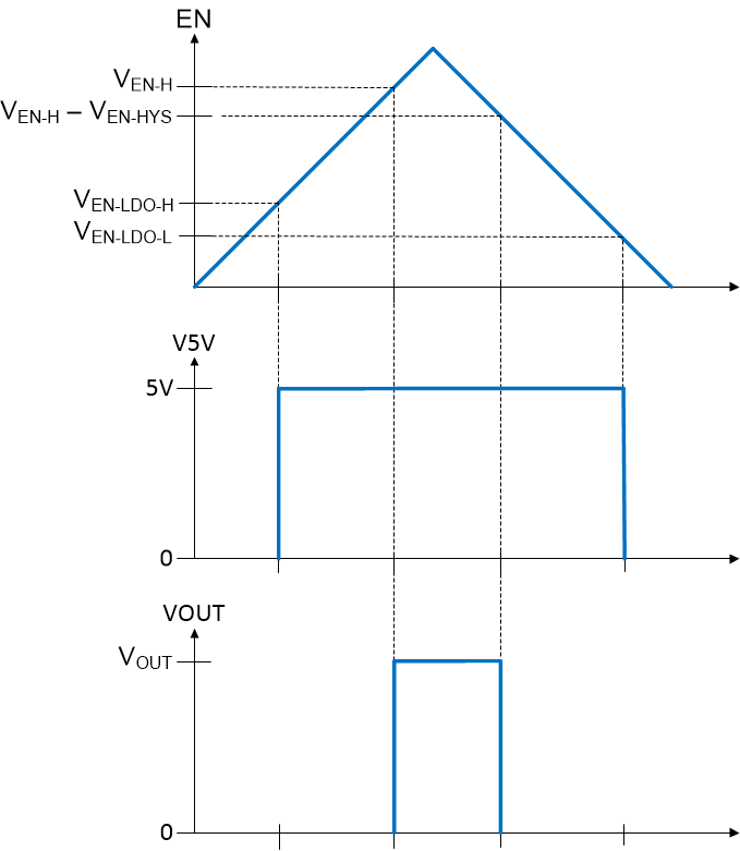
The voltage on the EN pin provides electrical ON/OFF control of the device. This input features precision thresholds, allowing the use of an external voltage divider to provide a programmable UVLO (see Section 7.3.6). Applying a voltage of VEN ≥ VEN-LDO_H causes the device to enter standby mode, powering the internal LDO, but not producing an output voltage. Increasing the EN voltage to VEN-H fully enables the device, allowing it to enter start-up mode and beginning the soft-start period. When the EN input is brought below VEN-H by VEN-HYS, the regulator stops running and enters standby mode. Further decrease in the EN voltage to below VEN-LDO-L completely shuts down the device. Figure 7-2 shows this behavior. The values for the various EN thresholds can be found in Section 6.5.
 Figure 7-2 Precision Enable Behavior
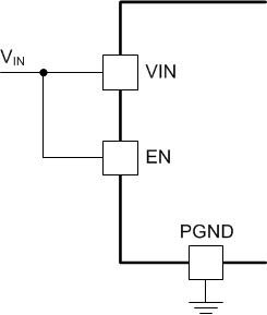
The EN pin cannot be open circuit or floating. The simplest way to enable the operation of the TPSM53602 is to connect the EN pin to VIN directly as shown in Figure 7-3. This allows self start-up of the TPSM53602 when VIN is within the operation range.
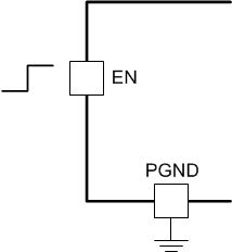
If an application requires controlling the EN pin, an external logic signal can be used to drive EN pin as shown in Figure 7-4. Applications using an open drain/collector device to interface with this pin require a pullup resistor to a voltage above the enable threshold.
 Figure 7-3 Enabling the Device
 Figure 7-4 Typical Enable Control