ZHCSKO0B December 2019 – September 2021 TPSM53602
PRODUCTION DATA
- 1 特性
- 2 应用
- 3 说明
- 4 Revision History
- 5 Pin Configuration and Functions
- 6 Specifications
-
7 Detailed Description
- 7.1 Overview
- 7.2 Functional Block Diagram
- 7.3
Feature Description
- 7.3.1 Adjusting the Output Voltage
- 7.3.2 Switching Frequency
- 7.3.3 Input Capacitors
- 7.3.4 Output Capacitors
- 7.3.5 Output On/Off Enable (EN)
- 7.3.6 Programmable Undervoltage Lockout (UVLO)
- 7.3.7 Power Good (PGOOD)
- 7.3.8 Light Load Operation
- 7.3.9 Voltage Dropout
- 7.3.10 Overcurrent Protection (OCP)
- 7.3.11 Thermal Shutdown
- 7.4 Device Functional Modes
- 8 Application and Implementation
- 9 Power Supply Recommendations
- 10Layout
- 11Device and Documentation Support
- 12Mechanical, Packaging, and Orderable Information
7.3.7 Power Good (PGOOD)
The TPSM53602 has a built-in power-good signal (PGOOD) which indicates whether the output voltage is within its regulation range. The PGOOD pin is an open-drain output that requires a pullup resistor to a nominal voltage source of 18 V or less. The internal 5-V LDO output (V5V pin) can be used as the pullup voltage source. A typical pullup resistor value is between 10 kΩ and 100 kΩ. The maximum recommended PGOOD sink current is 3 mA.
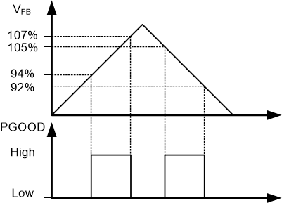
Once the output voltage rises above 94% of the set voltage, the PGOOD pin rises to the pullup voltage level. The PGOOD pin is pulled low when the output voltage drops lower than 92% or rises higher than 107% of the nominal set voltage. See Figure 7-6 for typical power-good thresholds.
 Figure 7-6 Power-good Flag