ZHCSKO1B December 2019 – September 2021 TPSM53603
PRODUCTION DATA
- 1 特性
- 2 应用
- 3 说明
- 4 Revision History
- 5 Pin Configuration and Functions
- 6 Specifications
-
7 Detailed Description
- 7.1 Overview
- 7.2 Functional Block Diagram
- 7.3
Feature Description
- 7.3.1 Adjusting the Output Voltage
- 7.3.2 Switching Frequency
- 7.3.3 Input Capacitors
- 7.3.4 Output Capacitors
- 7.3.5 Output On/Off Enable (EN)
- 7.3.6 Programmable Undervoltage Lockout (UVLO)
- 7.3.7 Power Good (PGOOD)
- 7.3.8 Light Load Operation
- 7.3.9 Voltage Dropout
- 7.3.10 Overcurrent Protection (OCP)
- 7.3.11 Thermal Shutdown
- 7.4 Device Functional Modes
- 8 Application and Implementation
- 9 Power Supply Recommendations
- 10Layout
- 11Device and Documentation Support
- 12Mechanical, Packaging, and Orderable Information
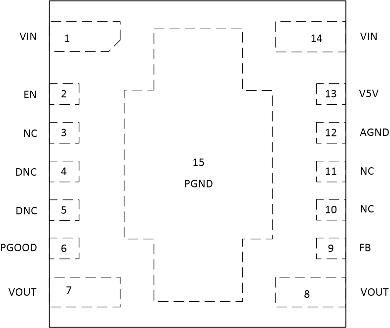
5 Pin Configuration and Functions
 Figure 5-1 15-Pin QFN RDA Package (Top
View)
Figure 5-1 15-Pin QFN RDA Package (Top
View)Table 5-1 Pin Functions
| PIN | TYPE | DESCRIPTION | |
|---|---|---|---|
| NO. | NAME | ||
| 12 | AGND | G | Analog ground. Zero voltage reference for internal references and logic. All electrical parameters are measured with respect to this pin. This pin must be connected to PGND at a single point. See Section 10 for a recommended layout. |
| 4, 5 | DNC | — | Do not connect. Do not connect these pins to ground, to another DNC pin, or to any other voltage. These pins are connected to internal circuitry. Each pin must be soldered to an isolated pad. |
| 2 | EN | I | Enable pin. This pin turns the converter on when pulled high and turns off the converter when pulled low. This pin can be connected directly to VIN. Do not float. This pin can be used to set the input under voltage lockout with two resistors. See Section 7.3.6. |
| 9 | FB | I | Feedback input. Connect the mid-point of the feedback resistor divider to this pin. Connect the upper resistor (RFBT) of the feedback divider to VOUT at the desired point of regulation. Connect the lower resistor (RFBB) of the feedback divider to AGND. |
| 3, 10, 11 | NC | — | Not connected. These pins are not connected to any circuitry within the module. It is recommended that these pins be connected to the PGND plane on the application board to enhance shielding and thermal performance. |
| 15 | PGND | G | Power ground. This is the return current path for the power stage of the device. Connect this pad to the input supply return, the load return, and the capacitors associated with the VIN and VOUT pins. See Section 10 for a recommended layout. |
| 6 | PGOOD | O | Power-good pin. Open-drain output that asserts low if the feedback voltage is not within the specified window thresholds. A 10-kΩ to 100-kΩ pullup resistor is required and can be tied to the V5V pin or other DC voltage less than 22 V. If not used, this pin can be left open or connected to PGND. |
| 1, 14 | VIN | I | Input supply voltage. Connect the input supply to these pins. Connect input capacitors between these pins and PGND in close proximity to the device. |
| 7, 8 | VOUT | O | Output voltage. These pins are connected to the internal output inductor. Connect these pins to the output load and connect external output capacitors between these pins and PGND. |
| 13 | V5V | O | Internal 5-V LDO output. Supplies internal control circuits. Do not connect to external loads. This pin can be used as logic supply for PGOOD pin. |