ZHCSNO2 September 2021 TPSM5601R5
PRODUCTION DATA
- 1 特性
- 2 应用
- 3 说明
- 4 Revision History
- 5 Device Comparison Table
- 6 Pin Configuration and Functions
-
7 Specifications
- 7.1 Absolute Maximum Ratings
- 7.2 ESD Ratings
- 7.3 Recommended Operating Conditions
- 7.4 Thermal Information
- 7.5 Electrical Characteristics
- 7.6 Typical Characteristics (VIN = 12 V)
- 7.7 Typical Characteristics (VIN = 24 V)
- 7.8 Typical Characteristics (VIN = 48 V)
- 7.9 Typical Characteristics (VIN = 60 V)
- 8 Detailed Description
- 9 Applications and Implementation
- 10Power Supply Recommendations
- 11Layout
- 12Device and Documentation Support
- 13Mechanical, Packaging, and Orderable Information
6 Pin Configuration and Functions
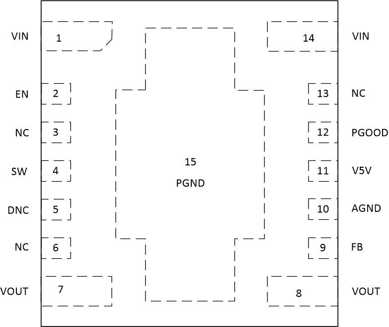
 Figure 6-1 15-Pin QFN RDA Package (Top
View)
Figure 6-1 15-Pin QFN RDA Package (Top
View)Table 6-1 Pin Functions
| PIN | TYPE(1) | DESCRIPTION | |
|---|---|---|---|
| NO. | NAME | ||
| 10 | AGND | G | Analog ground. Zero voltage reference for internal references and logic. All electrical parameters are measured with respect to this pin. This pin must be connected to PGND at a single point. See Section 11.2 for a recommended layout. |
| 5 | DNC | — | Do not connect. Do not connect this pin to ground, to another pin, or to any other voltage. This pin is connected to the internal bootstrap capacitor. This pin must be soldered to an isolated pad. |
| 2 | EN | I | Enable pin. This pin turns the converter on when pulled high and turns off the converter when pulled low. This pin can be connected directly to VIN. Do not float. This pin can be used to set the input undervoltage lockout with two resistors. See Section 8.3.4. |
| 9 | FB | I | Feedback input. Connect the mid-point of the feedback resistor divider to this pin. Connect the upper resistor (RFBT) of the feedback divider to VOUT at the desired point of regulation. Connect the lower resistor (RFBB) of the feedback divider to AGND. |
| 3, 6, 13 | NC | — | Not connected. These pins are not connected to any circuitry within the module. Leaving these pins unconnected to any other signal increases spacing near the high voltage pins (VIN, SW, EN, and DNC). However, if the high voltage spacing is not needed in the application, connecting these pins to the PGND plane can help enhance shielding and thermal performance. |
| 15 | PGND | G | Power ground. This is the return current path for the power stage of the device. Connect this pad to the input supply return, load return, and capacitors associated with the VIN and VOUT pins. See Section 11.2 for a recommended layout. |
| 12 | PGOOD | O | Power-good pin. Open-drain output that asserts low if the feedback voltage is not within the specified window thresholds. A 10-kΩ to 100-kΩ pullup resistor is required and can be tied to the V5V pin or other DC voltage less than 18 V. If not used, this pin can be left open or connected to PGND. |
| 4 | SW | O | Switch node. Do not place any external component on this pin or connect to any signal. |
| 1, 14 | VIN | I | Input supply voltage. Connect the input supply to these pins. Connect input capacitors between these pins and PGND in close proximity to the device. |
| 7, 8 | VOUT | O | Output voltage. These pins are connected to the internal output inductor. Connect these pins to the output load and connect external output capacitors between these pins and PGND. |
| 11 | V5V | O | Internal 5-V LDO output. Supplies internal control circuits. Do not connect to external loads. This pin can be used as logic supply for the PGOOD pin. |
(1) G = Ground, I = Input, O = Output