ZHCSP41 January 2022 TPSM5D1806E
PRODUCTION DATA
- 1 特性
- 2 应用
- 3 说明
- 4 Revision History
- 5 Pin Configuration and Functions
- 6 Specifications
-
7 Detailed Description
- 7.1 Overview
- 7.2 Functional Block Diagram
- 7.3
Feature Description
- 7.3.1 Adjustable Output Voltage
- 7.3.2 Frequency Selection
- 7.3.3 Minimum and Maximum Input Voltage
- 7.3.4 Recommended Settings
- 7.3.5 Device Mode Configuration
- 7.3.6 Input Capacitors
- 7.3.7 Minimum Required Output Capacitance
- 7.3.8 Ambient Temperature Versus Total Power Dissipation
- 7.3.9 Remote Sense
- 7.3.10 Enable (EN) and Undervoltage Lockout (UVLO)
- 7.3.11 Soft Start
- 7.3.12 Power Good
- 7.3.13 Safe Start-Up into Pre-Biased Outputs
- 7.3.14 BP5
- 7.3.15 Overcurrent Protection
- 7.3.16 Thermal Shutdown
- 7.4 Device Functional Modes
- 8 Application and Implementation
- 9 Power Supply Recommendations
- 10Layout
- 11Device and Documentation Support
- 12Mechanical, Packaging, and Orderable Information
7.3.7 Minimum Required Output Capacitance
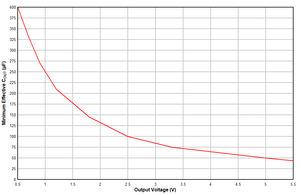
The TPSM5D1806E requires a minimum amount of ceramic output capacitance (per phase) depending on the output voltage setting. The amount of required output capacitance is shown in Figure 7-5 and is the amount of effective capacitance. The effects of DC bias and temperature variation must be considered when using ceramic capacitance. For ceramic capacitors, the package size, voltage rating, and dielectric material contributes to differences between the standard rated value and the actual effective value of the capacitance. When adding additional capacitance above the minimum, the capacitance can be ceramic type, low-ESR polymer type, or a combination of the two.
 Figure 7-5 Minimum Required Output Capacitance (per Phase)