ZHCSPT6D July 2023 – June 2024 TPSM8287A06 , TPSM8287A10 , TPSM8287A12 , TPSM8287A15
PRODUCTION DATA
- 1
- 1 特性
- 2 应用
- 3 说明
- 4 Device Options
- 5 Pin Configuration and Functions
- 6 Specifications
-
7 Detailed Description
- 7.1 Overview
- 7.2 Functional Block Diagram
- 7.3
Feature Description
- 7.3.1 Fixed-Frequency DCS-Control Topology
- 7.3.2 Forced-PWM and Power-Save Modes
- 7.3.3 Precise Enable
- 7.3.4 Start-Up
- 7.3.5 Switching Frequency Selection
- 7.3.6 Output Voltage Setting
- 7.3.7 Compensation (COMP)
- 7.3.8 Mode Selection / Clock Synchronization (MODE/SYNC)
- 7.3.9 Spread Spectrum Clocking (SSC)
- 7.3.10 Output Discharge
- 7.3.11 Undervoltage Lockout (UVLO)
- 7.3.12 Overvoltage Lockout (OVLO)
- 7.3.13 Overcurrent Protection
- 7.3.14 Power Good (PG)
- 7.3.15 Remote Sense
- 7.3.16 Thermal Warning and Shutdown
- 7.3.17 Stacked Operation
- 7.4 Device Functional Modes
- 7.5 Programming
- 8 Device Registers
-
9 Application and Implementation
- 9.1 Application Information
- 9.2 Typical Application
- 9.3 Typical Application Using Four TPSM8287Axx in Parallel Operation
- 9.4 Power Supply Recommendations
- 9.5 Layout
- 10Device and Documentation Support
- 11Revision History
- 12Mechanical, Packaging, and Orderable Information
7.3.10 Output Discharge
The device has an output discharge function which makes sure a defined ramp down of the output voltage when the device is disabled. The discharge stays on after the output is discharged. The output discharge function is enabled when DISCHEN = 1 in the CONTROL1 register.
If output discharge is enabled, the device discharges the output under the following conditions:
- A low level is applied to the EN pin
- SWEN = 0 in the CONTROL1 register
- A thermal shutdown event occurs
- An UVLO event occurs
- An OVLO event occurs
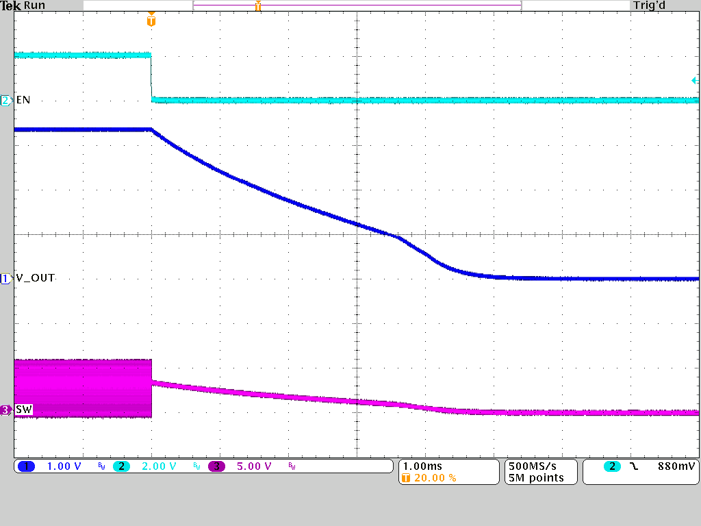
When the output voltage is above 900 mV (typical), the discharge is about 115 mA. Below 900 mV, the discharge is about 3.5 Ohm. Figure 7-17 shows an example of the typical discharge behavior.

| VIN = 5.0 V | IOUT = 0 mA | VOUT = 3.3 V discharge to 0 V |
The output discharge function is not available until the device has been enabled at least once after applying VIN. The output discharge functions until VIN drops to around 1.8 V.
In a stacked configuration, the discharge is always active in the secondary devices. Please refer to Table 7-6.