ZHCSOW9C october 2022 – july 2023 TPSM82912 , TPSM82913 , TPSM82913E
PRODUCTION DATA
- 1
- 1 特性
- 2 应用
- 3 说明
- 4 Revision History
- 5 Pin Configuration and Functions
- 6 Specifications
-
7 Detailed Description
- 7.1 Overview
- 7.2 Functional Block Diagram
- 7.3
Feature Description
- 7.3.1 Smart Config (S-CONF)
- 7.3.2 Device Enable (EN/SYNC)
- 7.3.3 Device Synchronization (EN/SYNC)
- 7.3.4 Spread Spectrum Modulation
- 7.3.5 Output Discharge
- 7.3.6 Undervoltage Lockout (UVLO)
- 7.3.7 Power-Good Output
- 7.3.8 Noise Reduction and Soft-Start Capacitor (NR/SS)
- 7.3.9 Current Limit and Short-Circuit Protection
- 7.3.10 Thermal Shutdown
- 7.4 Device Functional Modes
- 8 Application and Implementation
- 9 Device and Documentation Support
- 10Mechanical, Packaging, and Orderable Information
5 Pin Configuration and Functions
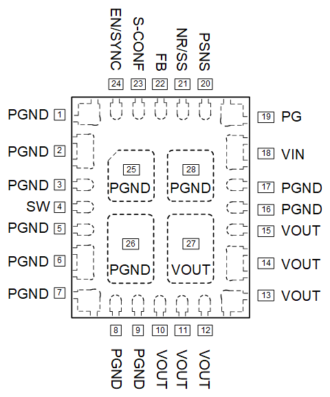
 Figure 5-1 28-Pin QFN RDU Package (Top View)
Table 5-1 Pin Functions
| PIN | I/O | DESCRIPTION | |
|---|---|---|---|
| NO. | NAME | ||
18 | VIN | I | Power supply input voltage pin |
| 1, 2, 3, 5, 6, 7, 8, 9, 16, 17, 25, 26, 28 | PGND | Power ground connection | |
10, 11, 12, 13, 14, 15, 27 | VOUT | O | Output connection. Connect recommended output capacitance from VOUT to PGND. |
4 | SW | NC | Switch pin of the power stage. Do not connect, leave floating. |
19 | PG | O | Open-drain power-good output. This pin is pulled to GND when VOUT is below the power-good threshold. It requires a pull-up resistor to output a logic high. It can be left open or tied to GND if not used. |
20 | PSNS | I | Power sense ground. Connect directly to the ground plane. |
21 | NR/SS | O | A capacitor connected to this pin sets the soft-start time and low frequency noise level of the device. |
22 | FB | I | Feedback pin of the device |
23 | S-CONF | O | Smart Configuration pin. This pin configures the operation modes of the device. See Table 7-1. |
24 | EN/SYNC | I | Enable/Disable pin including threshold-comparator. Connect to logic low to disable the device. Pull high to enable the device. This pin has an internal pull-down resistor of typically 500 kΩ when the device is disabled. Apply a clock to this pin to synchronize the device. |