ZHCSGE1A July   2017  – August 2017 TPSM84203 , TPSM84205 , TPSM84212

PRODUCTION DATA.  

  1. 特性
  2. 应用
  3. 说明
    1.     Device Images
      1.      简化应用
  4. 修订历史记录
  5. Pin Configuration and Functions
    1.     Pin Functions
  6. Specifications
    1. 6.1 Absolute Maximum Ratings
    2. 6.2 Recommended Operating Conditions
    3. 6.3 ESD Ratings
    4. 6.4 Thermal Information
    5. 6.5 Electrical Characteristics
    6. 6.6 Switching Characteristics
    7. 6.7 Typical Characteristics (VOUT = 3.3 V)
    8. 6.8 Typical Characteristics (VOUT = 5 V)
    9. 6.9 Typical Characteristics (VOUT = 12 V)
  7. Detailed Description
    1. 7.1 Overview
    2. 7.2 Functional Block Diagram
    3. 7.3 Feature Description
      1. 7.3.1 Input Capacitors
      2. 7.3.2 Output Capacitors
      3. 7.3.3 Drop-Out Voltage
      4. 7.3.4 Internal Soft-Start
      5. 7.3.5 Safe Startup into Pre-Biased Outputs
      6. 7.3.6 Over-Current Protection
      7. 7.3.7 Output Over-Voltage Protection
      8. 7.3.8 Thermal Shutdown
    4. 7.4 Device Functional Modes
      1. 7.4.1 Normal Operation
      2. 7.4.2 Eco-mode Operation
  8. Application and Implementation
    1. 8.1 Application Information
    2. 8.2 Typical Application
      1. 8.2.1 Design Requirements
      2. 8.2.2 Detailed Design Procedure
        1. 8.2.2.1 Custom Design With WEBENCH® Tools
        2. 8.2.2.2 Input and Output Capacitors
      3. 8.2.3 Application Curves
        1. 8.2.3.1 EMI
  9. Power Supply Recommendations
  10. 10Layout
    1. 10.1 Layout Guidelines
    2. 10.2 Layout Example
  11. 11器件和文档支持
    1. 11.1 器件支持
      1. 11.1.1 开发支持
        1. 11.1.1.1 使用 WEBENCH® 工具创建定制设计
    2. 11.2 相关链接
    3. 11.3 Receiving Notification of Documentation Updates
    4. 11.4 Community Resources
    5. 11.5 商标
    6. 11.6 静电放电警告
    7. 11.7 Glossary
  12. 12机械、封装和可订购信息

封装选项

机械数据 (封装 | 引脚)
散热焊盘机械数据 (封装 | 引脚)
订购信息

Typical Characteristics (VOUT = 5 V)

Typical characteristic data has been developed from actual products tested at 25°C. This data is considered typical for the device. Safe operating area curves were measured using a Texas Instruments evaluation module (EVM).
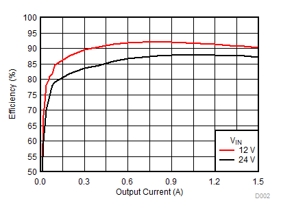
TPSM84203 TPSM84205 TPSM84212 5Vefficiency2.gif
VOUT = 5 V
Figure 6. Efficiency vs Output Current
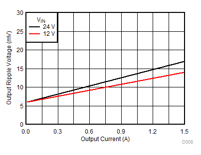
TPSM84203 TPSM84205 TPSM84212 5Vripple.gif
VOUT = 5 V COUT = 2x 47 µF
Figure 8. Ripple Voltage vs Output Current
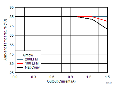
TPSM84203 TPSM84205 TPSM84212 SOA24Vto5V.gif
VOUT = 5 V VIN = 24 V
Figure 10. Safe Operating Area
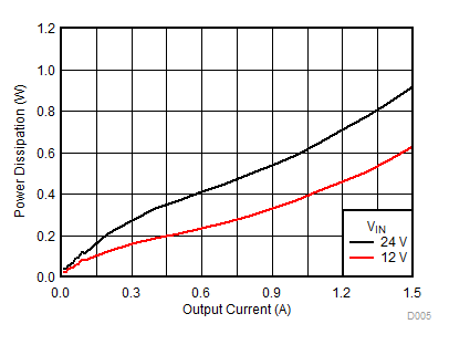
TPSM84203 TPSM84205 TPSM84212 5VPdis.gif
VOUT = 5 V
Figure 7. Power Dissipation vs Output Current
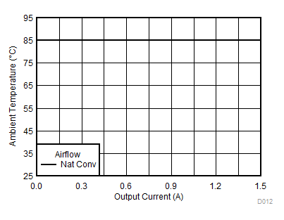
TPSM84203 TPSM84205 TPSM84212 SOA5Vflat.gif
VOUT = 5 V VIN ≤ 15 V
Figure 9. Safe Operating Area