ZHCSGE1A July 2017 – August 2017 TPSM84203 , TPSM84205 , TPSM84212
PRODUCTION DATA.
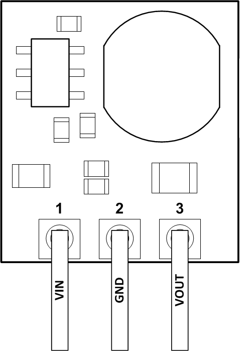
5 Pin Configuration and Functions
EAB Package
3-Pin Through-Hole
Top View

Pin Functions
| PIN | I/O | DESCRIPTION | |
|---|---|---|---|
| NAME | NO. | ||
| GND | 2 | Ground. This is the return current path for the power stage of the device. Connect this pin to the bypass capacitors associated with VIN and VOUT. | |
| VIN | 1 | I | Input Voltage. This pin supplies voltage to the control circuitry and power switches of the converter. Connect external bypass capacitors between this pin and GND. |
| VOUT | 3 | O | Output Voltage. This pin is connected to the internal output inductor. Connect this pin to the output load and connect external bypass capacitors between this pin and GND. |