ZHCSPU4A October 2023 – December 2023 TPSM843820
PRODUCTION DATA
- 1
- 1 特性
- 2 应用
- 3 说明
- 4 Pin Configuration and Functions
- 5 Specifications
-
6 Detailed Description
- 6.1 Overview
- 6.2 Functional Block Diagram
- 6.3
Feature Description
- 6.3.1 VIN Pins and VIN UVLO
- 6.3.2 Enable and Adjustable UVLO
- 6.3.3 Adjusting the Output Voltage
- 6.3.4 Switching Frequency Selection
- 6.3.5 Switching Frequency Synchronization to an External Clock
- 6.3.6 Ramp Amplitude Selection
- 6.3.7 Soft Start and Prebiased Output Start-Up
- 6.3.8 Mode Pin
- 6.3.9 Power Good (PGOOD)
- 6.3.10 Current Protection
- 6.3.11 Output Overvoltage and Undervoltage Protection
- 6.3.12 Overtemperature Protection
- 6.3.13 Output Voltage Discharge
- 6.4 Device Functional Modes
-
7 Application and Implementation
- 7.1 Application Information
- 7.2
Typical Applications
- 7.2.1
1.0-V Output, 1.5-MHz Application
- 7.2.1.1 Design Requirements
- 7.2.1.2
Detailed Design Procedure
- 7.2.1.2.1 Switching Frequency
- 7.2.1.2.2 Output Inductor Selection
- 7.2.1.2.3 Output Capacitor
- 7.2.1.2.4 Input Capacitor
- 7.2.1.2.5 Adjustable Undervoltage Lockout
- 7.2.1.2.6 Output Voltage Resistors Selection
- 7.2.1.2.7 Bootstrap Capacitor Selection
- 7.2.1.2.8 BP5 Capacitor Selection
- 7.2.1.2.9 PGOOD Pullup Resistor
- 7.2.1.2.10 Current Limit Selection
- 7.2.1.2.11 Soft-Start Time Selection
- 7.2.1.2.12 Ramp Selection and Control Loop Stability
- 7.2.1.2.13 MODE Pin
- 7.2.1.3 Application Curves
- 7.2.1
1.0-V Output, 1.5-MHz Application
- 7.3 Power Supply Recommendations
- 7.4 Layout
- 8 Device and Documentation Support
- 9 Revision History
- 10Mechanical, Packaging, and Orderable Information
6.3.3 Adjusting the Output Voltage
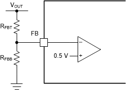
The output voltage is programmed with a resistor divider from the output (VOUT) to the FB pin shown in Figure 6-3. TI recommends to use 1% tolerance or better divider resistors. Starting with a fixed value for the bottom resistor, typically 10 kΩ, use Equation 3 to calculate the top resistor in the divider.
 Figure 6-3 FB Resistor Divider
Equation 3. 
