ZHCSHN7B February 2018 – April 2018 TPSM84624
PRODUCTION DATA.
- 1 特性
- 2 应用
- 3 说明
- 4 修订历史记录
- 5 Pin Configuration and Functions
- 6 Specifications
-
7 Detailed Description
- 7.1 Overview
- 7.2 Functional Block Diagram
- 7.3
Feature Description
- 7.3.1 Adjusting the Output Voltage
- 7.3.2 Switching Frequency (RT)
- 7.3.3 Synchronization (CLK)
- 7.3.4 Output On/Off Enable (EN)
- 7.3.5 Input Capacitor Selection
- 7.3.6 Output Capacitor Selection
- 7.3.7 TurboTrans (TT)
- 7.3.8 Undervoltage Lockout (UVLO)
- 7.3.9 Soft Start (SS/TR)
- 7.3.10 Sequencing (SS/TR)
- 7.3.11 Power Good (PGOOD)
- 7.3.12 Safe Start-Up Into Pre-Biased Outputs
- 7.3.13 Overcurrent Protection
- 7.3.14 Thermal Shutdown
- 7.4 Device Functional Modes
- 8 Application and Implementation
- 9 Power Supply Recommendations
- 10Layout
- 11器件和文档支持
- 12机械、封装和可订购信息
7.3.10 Sequencing (SS/TR)
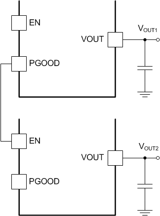
Many of the common power supply sequencing methods can be implemented using the SS/TR, EN, and PGOOD pins. The sequential method is illustrated in Figure 22 using two TPSM84624 devices. The PGOOD pin of the first device is coupled to the EN pin of the second device which enables the second power supply once the primary supply reaches regulation.
 Figure 22. Sequencing Schematic
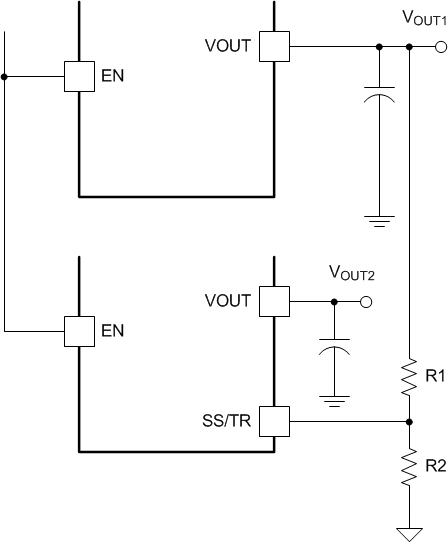
Simultaneous power supply sequencing can be implemented by connecting the resistor network of R1 and R2 shown in Figure 23 to the output of the power supply that needs to be tracked or to another voltage reference source. Use Equation 5 and Equation 6 to calculate the values of R1 and R2.
Equation 5. 

Equation 6. 

 Figure 23. Simultaneous Tracking Schematic